PCB Manufacturing: Unveiling the Heart of Modern Electronics
In the ever-evolving world of electronics, printed circuit boards (PCBs) stand as the unsung heroes that enable the seamless functioning of electronic devices we rely on daily. PCBs serve as the heart of modern electronics, providing the essential connectivity and support required for electronic components to work together harmoniously. FasTechCircuit This article delves into the fascinating world of PCB manufacturing, exploring the intricate processes that bring these vital components to life and their crucial role in shaping the technology landscape.
Classification: About FasTechCircuit ,More products
hot tags: PCB board manufacturer,PCB assembly
1. The Foundation of Electronics: Understanding PCBs
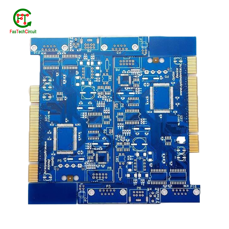
Printed circuit boards form the foundation of almost every electronic device we use. They are thin, flat boards made of non-conductive materials, such as fiberglass or composite epoxy, with a thin layer of conductive copper traces etched onto them. These copper traces create pathways that connect the electronic components and allow the flow of electrical signals, forming a functional electronic circuit.
2. PCB Design and Prototyping
The journey of PCB manufacturing begins with meticulous design and prototyping. Skilled PCB designers use specialized software to create intricate circuit layouts that suit the specific requirements of the electronic device. The design goes through multiple iterations to ensure its functionality, efficiency, and manufacturability.
Once the design is finalized, a prototype PCB is created for testing and validation. Prototyping enables engineers to identify and address potential issues before moving on to large-scale production.
3. Manufacturing Processes: From Raw Materials to Finished PCBs
PCB manufacturing involves several complex processes, each crucial to ensure the reliability and functionality of the final product:
3.1 Substrate Preparation: The process starts with the preparation of the substrate material, typically fiberglass-reinforced epoxy laminate. The substrate is cut into the desired size and shape to create the PCB.
3.2 Copper Cladding: The substrate is coated with a thin layer of copper on one or both sides. This copper cladding will form the conductive pathways on the PCB.
3.3 Photoengraving: A photosensitive layer called the photoresist is applied to the copper surface. The PCB design pattern is transferred onto the photoresist using UV light and a photo mask. The areas exposed to light become soluble, while the covered areas remain unaffected.
3.4 Etching: The exposed copper is chemically etched away, leaving behind the conductive traces as per the PCB design. This process creates the intricate pathways that connect the electronic components.
3.5 Drilling and Plating: Holes are drilled into the PCB to accommodate component leads and mounting. The holes are then plated with a thin layer of copper to create electrical connections.
3.6 Solder Mask and Silk Screen: A solder mask is applied to cover the copper traces, providing insulation and protection. A silk screen is also added to label component placement and other essential information.
3.7 Testing and Quality Control: The finished PCBs undergo rigorous testing to ensure their functionality and reliability. Advanced testing methods, such as Automated Optical Inspection (AOI), are used to identify any defects or faults.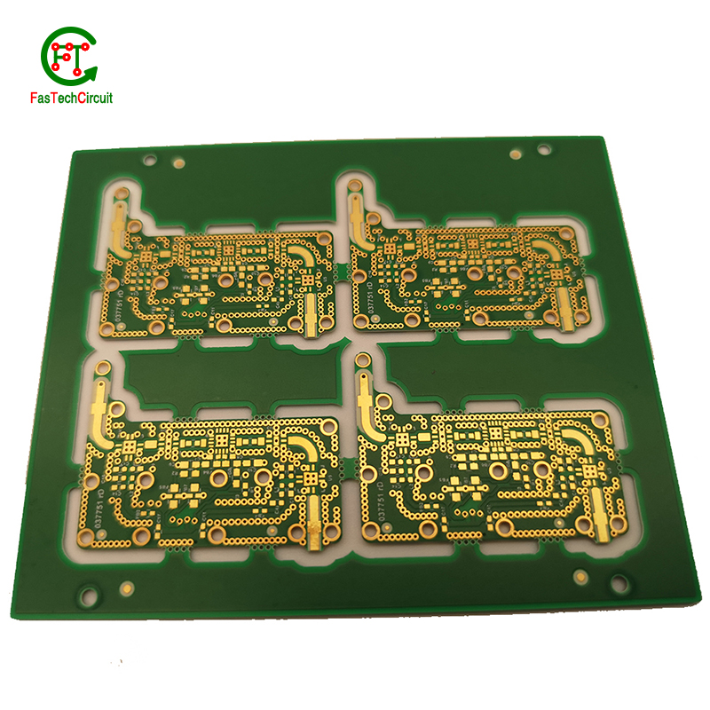
4. The Rise of Advanced PCB Technologies
As technology progresses, so do the capabilities of PCBs. Advanced PCB technologies, such as multilayer PCBs, flexible PCBs, and rigid-flex PCBs, have emerged to meet the demands of modern electronic devices. Multilayer PCBs, with multiple layers of copper traces, allow for more complex circuit designs and higher component density. Flexible PCBs enable the integration of electronics into curved or irregularly shaped surfaces. Rigid-flex PCBs combine the benefits of both rigid and flexible boards, offering a versatile solution for complex applications.
5. The Future of PCB Manufacturing
As technology continues to advance, the future of PCB manufacturing holds exciting possibilities. Industry experts anticipate further miniaturization of electronic components, leading to smaller and more powerful devices. Innovations in materials, such as organic PCBs and new conductive materials, may revolutionize PCB design and production processes. Additionally, sustainable practices and materials in PCB manufacturing will play an essential role in reducing the environmental impact of electronics.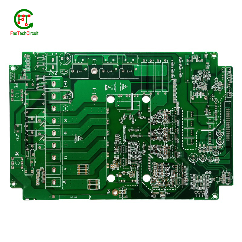
6. Conclusion: The Unsung Heroes of Electronics
PCB manufacturing serves as the backbone of modern electronics, enabling the seamless functioning of electronic devices we rely on in our daily lives. From smartphones to medical devices and from automotive systems to aerospace equipment, PCBs silently power our interconnected world. The precision, complexity, and adaptability of PCBs continue to shape the technology landscape, driving advancements in electronics and paving the way for a more connected and innovative future. As technology marches forward, the crucial role of PCB manufacturing as the heart of modern electronics will remain vital and continue to empower the devices that enrich our lives.
RELATED NEWS


pcb board manufacturing How To Contact US
PCB from 1 to 30 layers, HDI, Heavy Copper, Rigid-flex board with "pcb board manufacturing One-Stop" service.