How to calculate PCB assembly cost?
SMT is a popular assembly technique that involves the placement of tiny components onto a PCB board’s surface by melting solder paste with a reflow oven, creating a strong bond between the component and the board. On the other hand, THT involves drilling holes on the PCB board and inserting the components through the holes, followed by soldering on the opposite side, providing a strong mechanical connection.
There are many advantages to using PCB assembly in the production of electronic devices. One of the main benefits is the compact size of the final product. PCB boards take up less space than traditional wiring methods, making them ideal for compact devices such as smartphones and laptops. Additionally, the use of automated machines ensures a faster production process, reducing the time it takes to bring a product to the market.
PCB assembly also provides a high level of reliability and durability. The electronic components are securely attached to the board, preventing the risk of loose connections or damaged components. This results in products with a longer lifespan, reducing the need for repairs and replacements.
Moreover, PCB assembly allows for customization and flexibility in design. Different components can be easily added or removed from the board, making it easier to create customized products according to specific requirements. This makes PCB assembly a versatile and cost-effective solution for electronic product manufacturers.

The materials used in PCB assembly are also important factors to consider. High-quality materials, such as FR-4 fiberglass, ensure the durability and reliability of the assembled PCB, especially for electronic devices that require long-term use.
PCB assembly is crucial in the electronics industry as it enables the production of complex and compact electronic devices. This process also allows for easy and efficient repairs and upgrades to electronic products, making them more sustainable and cost-effective.
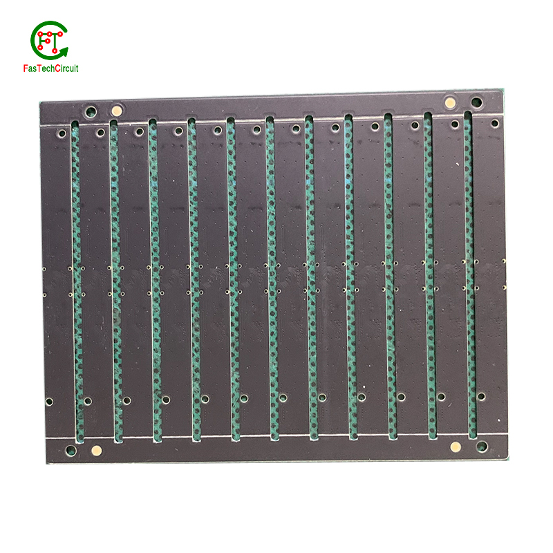
PCB assembly is the process of assembling electronic components onto printed circuit boards (PCBs). It plays a critical role in the production of various electronic devices, from household appliances to advanced industrial equipment. However, as technology advances and the demand for higher quality products increases, there are often concerns and questions regarding the PCB assembly process. In this FQA (Frequently Asked Questions) section, we will address some commonly asked questions to provide a better understanding of PCB assembly.
2.How to reduce PCB assembly cost?
3.Why are PCBs laminated?
4.Why is PCB assembly so expensive?
5.What is a PCB assembly?
6.Why is PCB poor?
1.What are the 17 common manufacturing processing steps in PCB production?
1. Design and Layout: The first step in PCB production is to create a design and layout of the circuit board using specialized software. 2. Material Selection: Once the design is finalized, the materials for the PCB are selected, including the substrate, copper foil, and solder mask. 3. Cutting: The substrate material is cut into the desired size and shape using a CNC machine or a laser cutter. 4. Drilling: Holes are drilled into the substrate for component placement and for creating electrical connections between layers. 5. Electroless Copper Deposition: A thin layer of copper is deposited on the substrate using a chemical process to create the conductive traces. 6. Imaging: A photosensitive layer called the resist is applied to the copper layer, and the PCB design is transferred onto it using a photomask and UV light. 7. Etching: The exposed copper is etched away using a chemical solution, leaving behind the desired circuit pattern. 8. Plating: A thin layer of copper is plated onto the remaining copper traces to increase their thickness and conductivity. 9. Solder Mask Application: A layer of solder mask is applied to the PCB to protect the copper traces and prevent short circuits. 10. Silkscreen Printing: The PCB is printed with component labels, logos, and other markings using a special ink called the silkscreen. 11. Surface Finish: A surface finish is applied to the exposed copper to protect it from oxidation and to improve solderability. 12. Electrical Testing: The PCB is tested for continuity and functionality using specialized equipment. 13. Component Placement: Electronic components such as resistors, capacitors, and ICs are placed on the PCB using automated pick-and-place machines. 14. Soldering: The components are soldered onto the PCB using a reflow oven or a wave soldering machine. 15. Inspection: The PCB is inspected for any defects or soldering errors using automated optical inspection (AOI) or manual inspection. 16. Final Testing: The assembled PCB is tested again to ensure that all components are functioning correctly. 17. Packaging and Shipping: The finished PCBs are packaged and shipped to the customer for use in electronic devices.
2.How to reduce PCB assembly cost?
1. Optimize the design: The first step to reducing PCB assembly cost is to optimize the design of the PCB. This includes reducing the size of the board, minimizing the number of layers, and simplifying the layout. This will not only reduce the cost of materials but also make the assembly process more efficient. 2. Use standard components: Using standard components instead of custom-made ones can significantly reduce the cost of PCB assembly. Standard components are readily available and can be purchased in bulk, which can result in cost savings. 3. Minimize the number of components: The more components on a PCB, the higher the assembly cost. Therefore, it is important to minimize the number of components by using multi-functional components or combining multiple functions into a single component. 4. Choose the right PCB manufacturer: It is important to choose a reliable and experienced PCB manufacturer who can provide high-quality assembly services at a competitive price. Get quotes from multiple manufacturers and compare their prices to find the best option. 5. Use surface mount technology (SMT): SMT is a more cost-effective assembly method compared to through-hole technology. It allows for faster assembly and reduces the need for manual labor, resulting in lower costs. 6. Opt for automated assembly: Automated assembly is faster, more accurate, and less labor-intensive compared to manual assembly. This can result in significant cost savings in the long run. 7. Plan for volume production: If you are planning to produce a large volume of PCBs, it is important to plan ahead and negotiate with the manufacturer for a bulk discount. 8. Reduce testing and inspection costs: Testing and inspection are important steps in the PCB assembly process, but they can also add to the overall cost. To reduce these costs, it is important to design the PCB with test points and perform thorough testing during the design phase to minimize the need for extensive testing during assembly. 9. Consider outsourcing: Outsourcing the PCB assembly to a specialized contract manufacturer can often be more cost-effective than doing it in-house. These manufacturers have the expertise, equipment, and resources to produce high-quality PCBs at a lower cost. 10. Continuously review and optimize the process: It is important to continuously review and optimize the PCB assembly process to identify any inefficiencies or areas for improvement. This can help reduce costs in the long run.
3.Why are PCBs laminated?
PCBs (printed circuit boards) are laminated for several reasons: 1. Protection: The lamination process adds a layer of protection to the PCB, making it more durable and resistant to damage from external factors such as moisture, dust, and heat. 2. Insulation: The lamination process also adds insulation to the PCB, preventing electrical shorts and ensuring proper functioning of the circuit. 3. Adhesion: Lamination helps to bond the different layers of the PCB together, ensuring that they stay in place and do not shift or separate during use. 4. Stability: Lamination helps to stabilize the PCB, preventing warping or bending that could affect the performance of the circuit. 5. Surface finish: The lamination process can also add a smooth and uniform surface finish to the PCB, making it easier to solder components onto the board. 6. Cost-effective: Lamination is a cost-effective way to manufacture PCBs, as it allows for multiple layers to be bonded together in a single process. 7. Customization: Lamination allows for the customization of PCBs, as different materials and thicknesses can be used to meet specific design requirements.
4.Why is PCB assembly so expensive?
1. High Cost of Materials: The materials used in PCB assembly, such as copper, solder, and components, can be expensive. The cost of these materials can significantly impact the overall cost of PCB assembly. 2. Complex Manufacturing Process: PCB assembly involves a complex manufacturing process that requires specialized equipment and skilled labor. This process can be time-consuming and labor-intensive, leading to higher costs. 3. Small Batch Production: PCB assembly is often done in small batches, which can increase the cost per unit. This is because the setup costs for each batch are the same, regardless of the batch size. 4. Quality Control: PCB assembly requires strict quality control measures to ensure that the final product meets the required standards. This involves testing and inspection at various stages of the manufacturing process, which can add to the cost. 5. Customization: Many PCB assemblies are customized to meet specific requirements, which can increase the cost. This is because the manufacturing process needs to be adjusted to accommodate the customization, leading to higher costs. 6. Design Complexity: The complexity of the PCB design can also impact the cost of assembly. More complex designs require more time and resources to manufacture, leading to higher costs. 7. Lead Time: PCB assembly often has a long lead time, which can increase the cost. This is because the longer the production time, the more resources and labor are required, leading to higher costs. 8. Location: The location of the PCB assembly facility can also impact the cost. Facilities in developed countries with higher labor and overhead costs may charge more for their services compared to facilities in developing countries. 9. Quality Standards: Some industries, such as aerospace and medical, have strict quality standards that must be met during PCB assembly. Meeting these standards can increase the cost of assembly. 10. Supply and Demand: The demand for PCB assembly can also impact the cost. If there is a high demand for PCB assembly, the cost may increase due to limited availability of resources and increased competition.
5.What is a PCB assembly?
A PCB assembly, also known as a printed circuit board assembly, is the process of attaching electronic components to a printed circuit board (PCB). This process involves soldering or otherwise attaching the components to the board, as well as testing and inspecting the assembly for functionality and quality. PCB assemblies are used in a wide range of electronic devices, from simple household appliances to complex computer systems. They are an essential part of the manufacturing process for electronic products.

6.Why is PCB poor?
There are a few reasons why PCB (Printed Circuit Board) may be considered poor: 1. Cost: PCBs can be expensive to manufacture, especially for small quantities or complex designs. This can make them less accessible for smaller companies or individuals. 2. Complexity: PCBs can be difficult to design and manufacture, especially for more complex circuits. This can lead to errors or defects in the final product. 3. Fragility: PCBs are made of thin layers of materials and can be easily damaged if mishandled or exposed to extreme conditions. This can make them less reliable and require frequent replacements. 4. Environmental impact: The production of PCBs involves the use of toxic chemicals and materials, which can have a negative impact on the environment if not properly disposed of. 5. Limited flexibility: PCBs are rigid and cannot be easily bent or shaped, making them less suitable for certain applications that require flexibility. 6. Limited customization: Once a PCB is manufactured, it is difficult to make changes or modifications to the design. This can be a disadvantage for products that require frequent updates or changes. 7. Limited scalability: PCBs are designed for specific applications and may not be easily scalable for different sizes or configurations. This can limit their use in different products or industries.
RELATED NEWS


pcb board manufacturing How To Contact US
PCB from 1 to 30 layers, HDI, Heavy Copper, Rigid-flex board with "pcb board manufacturing One-Stop" service.