what do you need to know about MULTILAYER PCB?
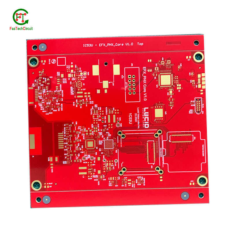
1. Definition: A Multilayer PCB (Printed Circuit Board) is a type of PCB that contains more than two layers of conductive material separated by insulating layers. It is used in electronic devices to provide compactness and high functionality.
2. Construction: A Multilayer PCB is constructed by laminating multiple layers of copper foil and insulating material together, which are then etched to create the required conductive paths.
3. Number of Layers: A Multilayer PCB typically consists of three or more layers, but can have up to hundreds of layers depending on the complexity of the circuit design.
4. Benefits: Multilayer PCB offers several advantages over traditional single or double layer PCB, such as increased functionality, higher component density, improved signal integrity, and reduced size and weight.
5. Applications: Multilayer PCB are widely used in various electronic devices and industries such as telecommunications, aerospace, medical equipment, automotive, and consumer electronics.
6. Types of Multilayer PCB: There are several types of Multilayer PCB, including rigid, flex, and rigid-flex PCB, each with its own unique properties and applications.
7. Design Considerations: Designing a Multilayer PCB requires careful consideration of factors such as power and signal integrity, thermal management, and component placement to ensure optimal performance.
8. Materials Used: The materials used in Multilayer PCB are chosen based on their dielectric properties, thermal conductivity, and compatibility with the manufacturing process. Common materials include FR-4, polyimide, and PTFE.
9. Manufacturing Process: The manufacturing process of Multilayer PCB involves several steps, including layer alignment and lamination, drilling, plating, etching, and finishing.
10. Challenges: Multilayer PCB pose some challenges during manufacturing, such as registration errors, delamination, and reliability issues, which require specialized techniques and equipment to address.
11. Cost: The cost of Multilayer PCB is higher than single or double-sided PCB due to the complexity of the manufacturing process and the amount of materials used.
12. Testing and Inspection: Multilayer PCB undergo rigorous testing and inspection processes to ensure that the final product meets the required specifications and quality standards.
13. Design Software: Various CAD software is used to design Multilayer PCB, allowing for accurate placement of components, efficient routing, and simulation of the circuit's performance.
14. Prototyping: Prototyping of Multilayer PCB is necessary to identify any design flaws or manufacturing issues before mass production, reducing the risk of costly mistakes.
15. High-Frequency Applications: Multilayer PCB are ideal for high-frequency applications due to their low signal loss, reduced electromagnetic interference, and controlled impedance.
16. Assembly: The assembly of Multilayer PCB requires specialized techniques such as reflow soldering and surface mount technology (SMT) to ensure precise positioning of components.
17. Stacked Vias: Stacked vias are used in Multilayer PCB to connect two or more different layers, conserving space and enhancing signal performance.
18. Blind and Buried Vias: Blind and buried vias are used in Multilayer PCB to connect inner layers without passing through the entire board, allowing for a higher component density and less signal interference.
19. Denser Component Placement: The compact size of Multilayer PCB allows for denser placement of components, reducing the length of signal paths and improving the overall efficiency of the circuit.
20. Environmental Considerations: The materials used in Multilayer PCB are environmentally friendly and can be recycled, reducing the impact on the environment compared to single-layer PCB.
Our rigid-flex multilayer PCB offers the ultimate combination of functionality and durability. With both rigid and flexible layers, this PCB can be bent and twisted to fit into tight spaces, while still maintaining the reliability of rigid boards. Its multilayer design allows for increased circuit density, making it an ideal choice for compact and lightweight electronic devices. Whether you need a prototype or a large-scale production, our rigid-flex multilayer PCB can provide the flexibility and durability your project needs.
2.What is the process for manufacturing a multilayer PCB?
3.Is it possible to repair a damaged multilayer PCB?
4.Can multilayer PCBs be used for high-frequency applications?
5.Can I use multilayer PCBs for high-speed digital applications?
6.Can I use multilayer PCBs in harsh environments?
1.What is the difference between a multilayer and a flex PCB?
A multilayer PCB is rigid and does not allow bending, while a flex PCB is made of flexible materials and allows for bending and twisting. Both types can have multiple conductive layers.
2.What is the process for manufacturing a multilayer PCB?
The process for manufacturing a multilayer PCB involves several steps, including layer stackup, drilling, plating, etching, and solder masking. It also involves inspections and testing to ensure quality and accuracy.
3.Is it possible to repair a damaged multilayer PCB?
In most cases, damaged multilayer PCBs cannot be repaired and would need to be replaced. However, it is possible to repair minor damage, such as a broken trace or damaged via.

4.Can multilayer PCBs be used for high-frequency applications?
Yes, multilayer PCBs are suitable for high-frequency applications due to their reduced signal loss and improved signal integrity.
5.Can I use multilayer PCBs for high-speed digital applications?
Yes, with proper design and manufacturing techniques, multilayer PCBs can be suitable for high-speed digital applications such as computer motherboards and network hardware.
6.Can I use multilayer PCBs in harsh environments?
Yes, with the use of appropriate materials and coatings, multilayer PCBs can be made to withstand harsh environments, such as high temperatures, moisture, and chemicals.

RELATED NEWS


pcb board manufacturing How To Contact US
PCB from 1 to 30 layers, HDI, Heavy Copper, Rigid-flex board with "pcb board manufacturing One-Stop" service.