Exploring the advantages of Surface Mount Technology (SMT)
FPC wiring structures are usually divided into single-layer, double-layer and multi-layer structures. Multi-layer structures can effectively reduce the size of circuit boards and improve wiring efficiency, and are often used in the design of high-density and complex circuits.
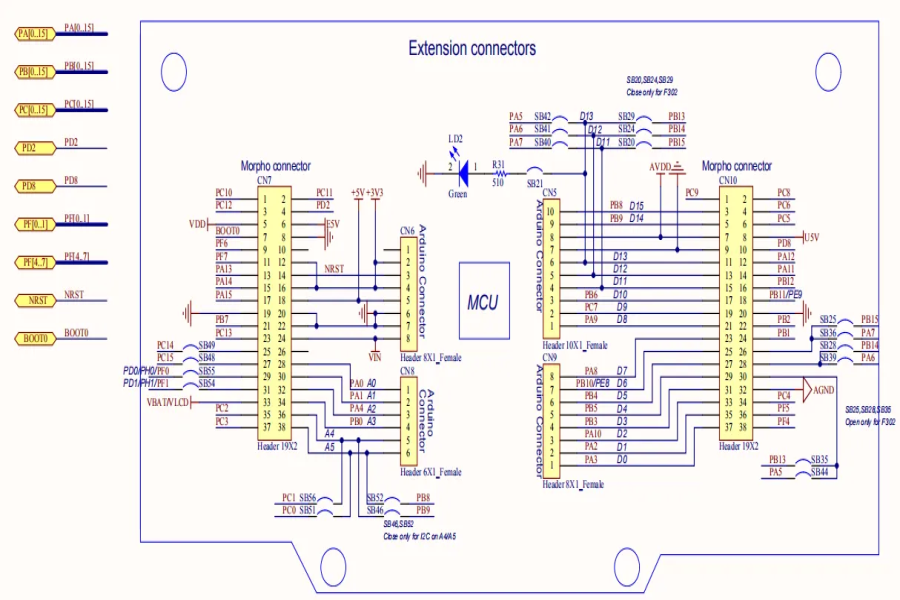
Optimizing PCB layout: the key to improving circuit performance
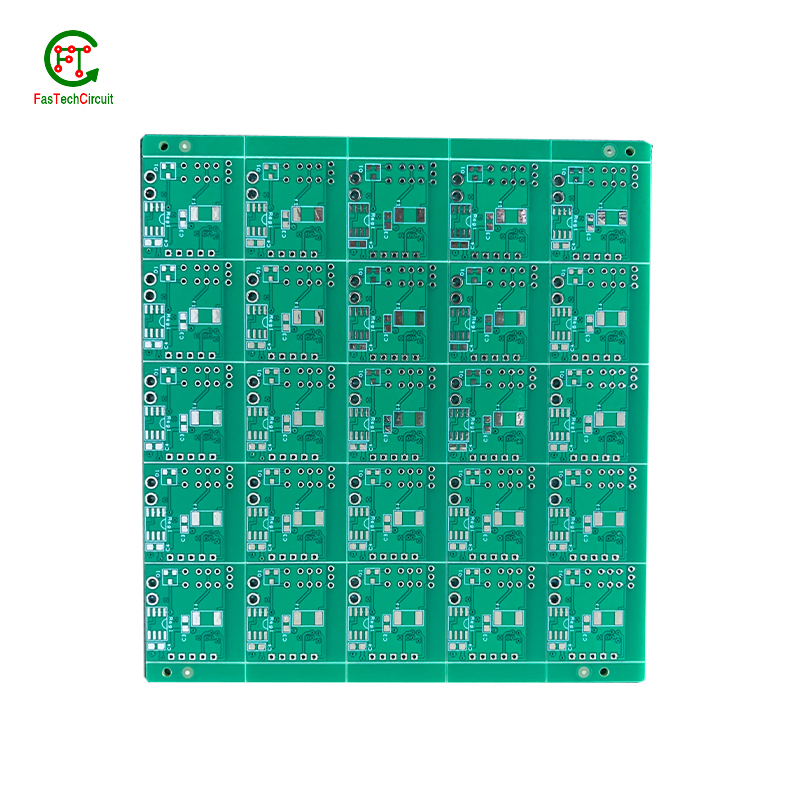
The PCB materials and trace routing used in our products are carefully selected and optimized to maintain low impedance, providing efficient signal transmission and minimizing electromagnetic interference.
Our PCB products are designed and manufactured to ensure high reliability under various operating conditions, minimizing the risk of failure and downtime.
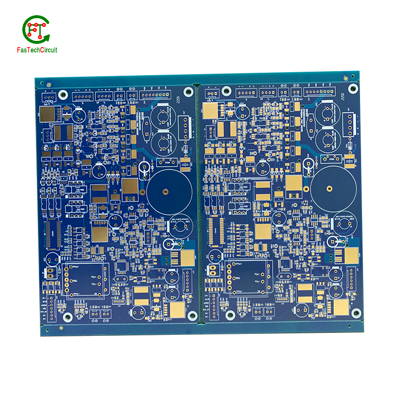
PCB--An Ultimate FAQ Guide.
2.How much voltage can PCB products withstand?
3.How is the circuit layout of PCB products designed?
4.About the scale of PCB factory
5.Do PCB products have radiation anti-interference capabilities?
6.About PCB overseas warehouse
7.About PCB inventory
8.About PCB raw materials
9.About PCB origin
10.About PCB origin
11.Does the PCB have radio frequency shielding properties?
12.What electronic components can this PCB product support?
13.What is the temperature range of PCB products?
14.What is the difference between PCB FasTechCircuit vs PCB Biostar vs PCB EVGA
15.Do PCB products have assembly functions?
16.Does PCB have the ability to resist electromagnetic interference?
17.Do PCB products have anti-static functions?
18.About PCB patent
19.Does the PCB have special anti-corrosion treatment?
1.Does the PCB have special anti-seismic design?
PCB (Printed Circuit Board) products typically do not have special anti-seismic designs as their primary function is to provide electrical connections and support for electronic components. Anti-seismic considerations are generally addressed at the system level in applications like industrial equipment, automotive electronics, or aerospace systems, where the entire system's design may incorporate anti-seismic measures to ensure stability and functionality during mechanical stress or vibrations. While PCBs themselves are not designed for anti-seismic purposes, they are integrated into systems that may have such protection in place to prevent damage or malfunction during seismic events.
2.How much voltage can PCB products withstand?
The voltage that PCB (Printed Circuit Board) products can withstand varies depending on several factors, including the design, materials, and intended application. PCBs are typically designed to withstand voltages ranging from a few volts to several hundred volts. Low-power electronic devices may have PCBs that can handle lower voltages, while high-power applications, such as power distribution or industrial equipment, may require PCBs designed to withstand higher voltages. Designers consider factors like insulation, spacing, and dielectric strength when determining the voltage tolerance of a PCB to ensure safe and reliable operation within its specified limits.
3.How is the circuit layout of PCB products designed?
The design of the circuit layout for PCB (Printed Circuit Board) products is a meticulous process that involves the placement and interconnection of electronic components to create a functional circuit. Designers use specialized software to arrange components on the board, optimize signal flow, and ensure efficient use of space. Factors like component placement, signal traces, power distribution, and signal integrity are considered during the design process. The goal is to create an organized and efficient layout that minimizes signal interference, maximizes functionality, and meets the specific requirements of the electronic system. The final circuit layout is a critical aspect of PCB design, ensuring the reliable performance of the electronic device or system.
4.About the scale of PCB factory
A PCB factory, also known as a printed circuit board factory, is a manufacturing facility that specializes in the production of printed circuit boards. These are used in a wide range of electronic devices, from smartphones and laptops to cars and airplanes. These factories vary in scale, with some producing small volumes for niche markets, while others are large operations that mass-produce PCBs for mainstream electronics companies. The scale of a PCB factory can be measured by its annual production output, the number of employees, and the size of its production facility. The larger the scale of a PCB factory, the more advanced and complex its production processes are likely to be, allowing it to produce high-quality boards in large quantities.
5.Do PCB products have radiation anti-interference capabilities?
PCB (Printed Circuit Board) products can be designed with radiation anti-interference capabilities to reduce the risk of electromagnetic interference (EMI) and improve the overall performance of electronic systems. Various techniques are employed to minimize EMI, including proper grounding, signal routing, shielding, and the use of filtering components. Additionally, some PCBs may incorporate specialized designs to mitigate radiation and reduce interference with other electronic components. These anti-interference measures are essential in applications where EMI can disrupt signal integrity and affect the functionality of sensitive electronic devices, ensuring that PCB products operate reliably in the presence of electromagnetic radiation.
6.About PCB overseas warehouse
A PCB overseas warehouse is a storage facility strategically located in a different country than the manufacturer's main facility, allowing for easy shipment and delivery of printed circuit boards (PCBs) to international customers. This provides numerous benefits including faster shipping times, reduced shipping costs, and improved customer service. These warehouses serve as a key component in the global supply chain of PCBs, facilitating efficient and timely distribution of products to meet the demands of a global market.
7.About PCB inventory
PCB inventory, or printed circuit board inventory, refers to the collection of all available PCBs (printed circuit boards) in stock for a particular company or organization. These PCBs are crucial components in the production of electronic devices and serve as the foundation for the electrical connections between various components. Maintaining an efficient and well-managed PCB inventory is essential for companies to meet the demand for their products, reduce production costs, and stay competitive in the market. Regular inventory checks, tracking of usage, and proper storage and handling of PCBs are key factors in managing a successful PCB inventory.
8.About PCB raw materials
PCB (printed circuit board) raw materials refer to the materials used to manufacture PCBs, which serve as the backbone of electronic devices. These materials can include various types of substrates, such as fiberglass, ceramic, and plastic, as well as copper, tin, and other metals for the conductive layers and traces. Other essential components include solder masks, silkscreen printing inks, and metal finishes. The selection of these raw materials is crucial in determining the quality, durability, and performance of the final PCB product. Advances in technology have led to the development of new and improved raw materials, allowing for more compact and efficient PCB designs.
9.About PCB origin
Printed circuit boards (PCBs) have a rich history, dating back to the early 20th century. They were first developed as a replacement for complicated, hand-wired circuits in radio sets and are now an integral part of modern electronics. PCBs originated through the evolution of various technologies and have undergone significant advancements in design, materials, and production methods over the years. Today, they are widely used in a diverse range of industries, from consumer electronics to aerospace and automotive, making them an essential component in our daily lives.
10.About PCB origin
PCB, short for Printed Circuit Board, is one of the essential components in electronic devices. It serves as a foundation and support for electronic components, allowing them to be connected and work together. The origin of PCB can be traced back to the early 20th century when people found a need to create a more efficient and reliable way to connect, mount, and organize electronic components. Over time, with the development of technology and manufacturing processes, PCB has become an integral part of modern electronic devices, making our daily lives more convenient and connected. Today, PCBs are widely used in various industries, from consumer electronics to medical equipment, highlighting their critical role and contribution to the advancement of technology.
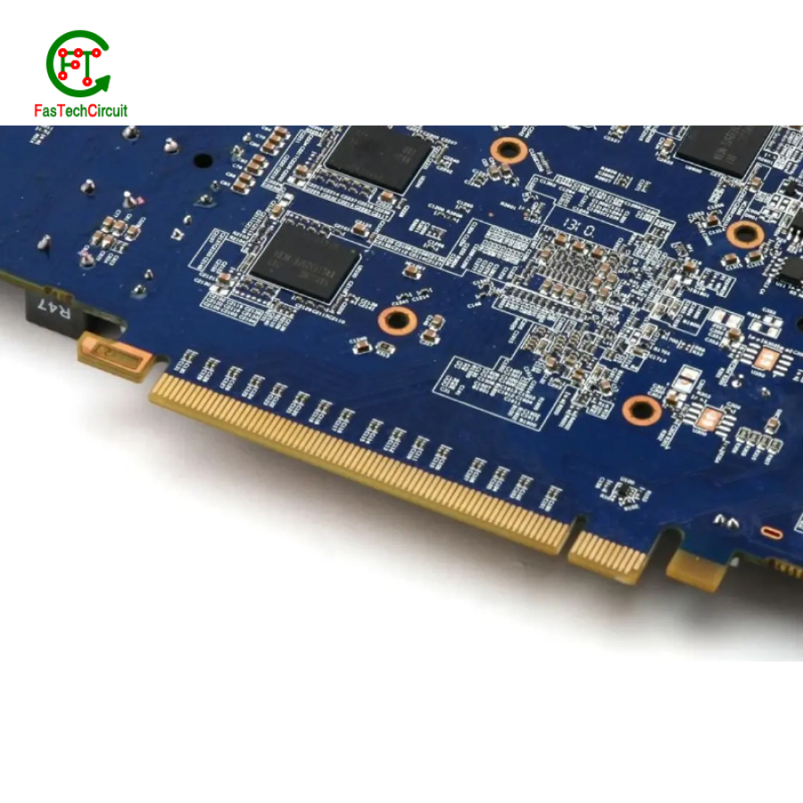
11.Does the PCB have radio frequency shielding properties?
PCB (Printed Circuit Board) products can be designed with radio frequency (RF) shielding properties, but this depends on the specific design requirements of the application. RF shielding is typically achieved through the use of shielding materials, such as metal cans or shields, placed over sensitive components or sections of the PCB. These shields are designed to block or attenuate electromagnetic interference at RF frequencies. The shielding effectiveness of a PCB is determined by its design, materials, and the presence of shielding components. PCBs themselves may not inherently have RF shielding properties, but they are a part of the overall system design that incorporates RF shielding when necessary to protect against interference.
12.What electronic components can this PCB product support?
The capabilities of this PCB (Printed Circuit Board) product extend to supporting a wide array of electronic components. These components include but are not limited to integrated circuits (ICs), microcontrollers, resistors, capacitors, diodes, transistors, connectors, and various sensors. The PCB's design and layout are tailored to accommodate these components and establish electrical connections between them. This versatility enables the PCB to be used in a broad spectrum of electronic devices and systems, where it acts as the central hub for component integration and electrical functionality.
13.What is the temperature range of PCB products?
The temperature range of PCB (Printed Circuit Board) products can vary significantly depending on their design and the materials used. PCBs are typically specified with an operating temperature range, which indicates the temperatures at which they can safely and reliably function. Common temperature ranges for PCBs in standard electronic devices are -40°C to 85°C or 0°C to 70°C. However, for specialized applications, such as industrial or automotive electronics, PCBs may have wider operating temperature ranges, extending from -40°C to 125°C or higher. The choice of temperature range depends on the intended application and environmental conditions in which the PCB will be used, ensuring that it can withstand the required temperature extremes without degradation in performance.
14.What is the difference between PCB FasTechCircuit vs PCB Biostar vs PCB EVGA
The choice between these manufacturers should be based on your specific project requirements. PCB FasTechCircuit is ideal for fast prototyping, while PCB Biostar and PCB EVGA are trusted options for high-quality components in computer hardware, with EVGA specifically known for its gaming-oriented graphics cards. Your decision should align with the goals and needs of your project.
15.Do PCB products have assembly functions?
PCB (Printed Circuit Board) products do not inherently have assembly functions themselves but are designed to support the assembly of electronic components. PCBs serve as the foundational platform for mounting and interconnecting various electronic parts, such as resistors, capacitors, integrated circuits, and connectors. The assembly of these components onto the PCB is a critical part of the manufacturing process of electronic devices. The design of the PCB includes features like component footprints, solder pads, and traces to facilitate the precise placement and soldering of components. While PCBs are not responsible for the assembly process, their design is tailored to enable the efficient and reliable assembly of electronic components.
16.Does PCB have the ability to resist electromagnetic interference?
PCB (Printed Circuit Board) products can be designed to resist electromagnetic interference (EMI) through various methods and features. EMI shielding, grounded planes, and controlled impedance routing are some common techniques used to mitigate the impact of EMI. PCB design and layout play a crucial role in minimizing EMI susceptibility and emissions. Additionally, the selection of materials and components can influence the PCB's EMI resistance. Proper grounding, signal isolation, and use of EMI shielding materials can help ensure that PCBs perform well in EMI-prone environments. The level of EMI resistance depends on the design and materials used, making it an important consideration in applications where EMI can affect electronic performance.
17.Do PCB products have anti-static functions?
PCB (Printed Circuit Board) products themselves do not typically have inherent anti-static functions. However, anti-static precautions are essential during the manufacturing and handling of PCBs. Static electricity can potentially damage sensitive electronic components on a PCB. To mitigate this risk, anti-static measures such as using anti-static workstations, wearing anti-static garments, and using anti-static tools and packaging materials are employed when working with PCBs. These precautions help prevent electrostatic discharge (ESD) and protect the integrity of the components and the PCB itself, ensuring that the final product functions reliably in electronic systems.
18.About PCB patent
PCB patent is a form of intellectual property protection that grants inventors and companies the exclusive right to produce and sell printed circuit boards (PCBs) with unique designs, functions, or processes. It serves as a means to encourage innovation and reward originality in the field of electronic circuitry and technology. PCB patents can cover a wide range of aspects, such as layout designs, fabrication methods, and manufacturing processes. However, in order to obtain a PCB patent, the design or process must meet specific criteria, including being novel, non-obvious, and useful. This type of patent is essential for companies and individuals in the electronics industry to protect their ideas and prevent others from copying or profiting from their innovations. By securing a PCB patent, inventors and companies can have a competitive advantage in the market and ensure the long-term success of their products.
19.Does the PCB have special anti-corrosion treatment?
PCB (Printed Circuit Board) products can undergo special anti-corrosion treatments to enhance their durability and resistance to environmental factors. Anti-corrosion treatments typically involve the application of conformal coatings, which create a protective layer over the PCB to shield it from moisture, humidity, and corrosive elements. These coatings act as a barrier against oxidation and chemical corrosion, preserving the integrity of the PCB components and connections. The choice to apply anti-corrosion treatment depends on the specific application and the potential exposure to corrosive agents, ensuring that the PCB remains reliable and functional in challenging conditions.
RELATED NEWS
pcb board manufacturing How To Contact US
PCB from 1 to 30 layers, HDI, Heavy Copper, Rigid-flex board with "pcb board manufacturing One-Stop" service.


