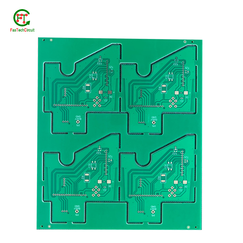
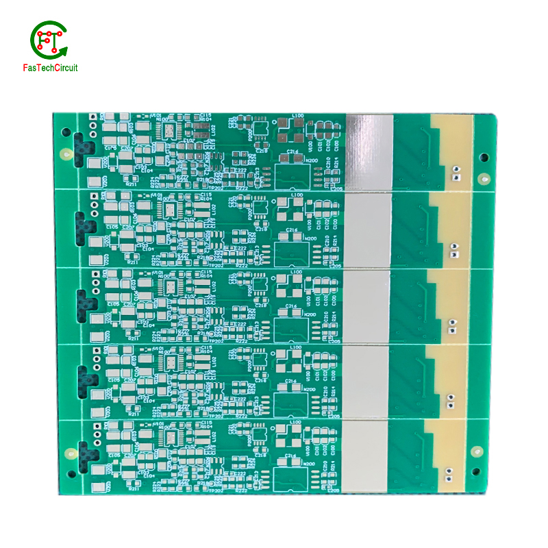
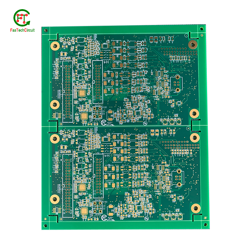
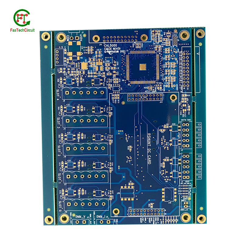
Why is PCB assembly important?
Another important aspect of PCB assembly is the efficient utilization of space. With the continuous advancement of technology, electronic products are becoming smaller and more compact. As a result, PCB assembly must maximize the use of surface area on the board, while still maintaining the necessary spacing and connections between components.
In addition, the use of surface mount technology has revolutionized the PCB assembly process. This technique allows for components to be mounted directly onto the surface of the board, rather than being inserted through holes. This not only allows for smaller and more efficient designs, but also facilitates automated assembly processes.
Quality control is also a crucial aspect of PCB assembly. With the complexity of modern electronic products, it is essential to ensure that all components are assembled correctly and functioning as intended. This requires a combination of visual inspection, functional testing, and specialized equipment to detect any defects or errors.
Furthermore, advancements in PCB assembly technology have also enabled the production of more complex and high-density products. This includes the use of multi-layered boards, where components are mounted on multiple layers for increased functionality and compactness.
In addition to its technical attributes, PCB assembly also plays a significant role in the cost and time efficiency of electronic product manufacturing. With automated assembly processes and efficient space utilization, the production time and cost can be significantly reduced, ultimately leading to higher profit margins for manufacturers.

PCB assembly is a critical part of the electronic manufacturing process. The assembly of a PCB involves the use of a variety of components, including passive and active components, which are carefully placed and soldered to create an electronic circuit. Additional processes such as cleaning, coating, and testing are also carried out to ensure the quality and durability of the PCB.
PCB assembly is crucial in the electronics industry as it enables the production of complex and compact electronic devices. This process also allows for easy and efficient repairs and upgrades to electronic products, making them more sustainable and cost-effective.

PCB assembly is the process of assembling electronic components onto printed circuit boards (PCBs). It plays a critical role in the production of various electronic devices, from household appliances to advanced industrial equipment. However, as technology advances and the demand for higher quality products increases, there are often concerns and questions regarding the PCB assembly process. In this FQA (Frequently Asked Questions) section, we will address some commonly asked questions to provide a better understanding of PCB assembly.
2.What is PCB assembly main?
3.What is the most commonly used PCB material?
4.What are the final processing steps in PCB assembly?
5.How is PCB thickness measured?
6.How do you calculate PCB size?
7.Why is PCB assembly important?
8.Can I clean PCB with water?
1.How many layers is a PCB?
The number of layers in a PCB (printed circuit board) can vary depending on the complexity and functionality of the circuit. However, most PCBs typically have between 1 and 12 layers. Some high-end or specialized PCBs may have more than 12 layers.
2.What is PCB assembly main?
PCB assembly, also known as printed circuit board assembly, is the process of attaching electronic components to a printed circuit board (PCB). This is a crucial step in the manufacturing of electronic devices, as it allows for the creation of a functional and operational circuit board. The main purpose of PCB assembly is to connect the electronic components to the PCB in a way that allows for the flow of electricity and the proper functioning of the device. This process involves various techniques such as soldering, surface mount technology, and through-hole technology. PCB assembly is a complex and precise process that requires specialized equipment and skilled technicians to ensure the quality and reliability of the final product.
3.What is the most commonly used PCB material?
The most commonly used PCB material is FR-4 (Flame Retardant 4), which is a type of fiberglass epoxy laminate. It is widely used due to its high strength, good electrical insulation properties, and low cost.
4.What are the final processing steps in PCB assembly?
1. Solder Paste Inspection (SPI): This step involves using a machine to inspect the solder paste deposits on the PCB before components are placed. 2. Pick and Place: In this step, automated machines are used to accurately place surface mount components onto the PCB. 3. Reflow Soldering: The PCB is then passed through a reflow oven where the solder paste is melted and the components are soldered onto the board. 4. Automated Optical Inspection (AOI): After reflow soldering, the PCB is inspected using a machine to detect any defects or errors in component placement or solder joints. 5. Through-Hole Component Insertion: Through-hole components, such as connectors and switches, are manually inserted into the PCB. 6. Wave Soldering: The PCB is passed through a wave soldering machine where the through-hole components are soldered onto the board. 7. Cleaning: The PCB is cleaned to remove any flux residue or other contaminants that may affect its performance. 8. Testing: The assembled PCB is then tested to ensure that all components are functioning correctly and the board meets the required specifications. 9. Final Inspection: A final visual inspection is performed to check for any defects or errors that may have been missed during the previous steps. 10. Packaging and Shipping: Once the PCB has passed all inspections and tests, it is packaged and shipped to the customer.

5.How is PCB thickness measured?
PCB thickness is typically measured in millimeters (mm) or mils (1 mil = 0.001 inches). It can be measured using a caliper or a thickness gauge specifically designed for PCBs. The measurement is taken from the top surface of the PCB to the bottom surface, including any copper layers, solder mask, and other coatings. The thickness can vary depending on the number of layers, materials used, and the manufacturing process.
6.How do you calculate PCB size?
To calculate the size of a PCB (printed circuit board), you will need to know the dimensions of the components that will be mounted on the board, as well as the spacing and placement of the components. You will also need to consider the size of the board itself, including any margins or borders. 1. Determine the dimensions of the components: Measure the length and width of each component that will be mounted on the PCB. This includes any integrated circuits, connectors, resistors, capacitors, etc. 2. Calculate the spacing between components: Determine the minimum spacing required between components to avoid interference or short circuits. This will depend on the size and type of components being used. 3. Add the spacing to the component dimensions: Add the spacing to the length and width of each component to determine the total size of each component on the PCB. 4. Determine the size of the board: Decide on the size of the PCB itself, including any margins or borders. This will depend on the size and number of components, as well as the desired layout and design. 5. Arrange the components on the board: Use a PCB design software or physical layout to arrange the components on the board. Make sure to leave enough space between components to avoid interference or short circuits. 6. Calculate the total size of the PCB: Add the dimensions of each component and the spacing between them to determine the total size of the PCB. 7. Consider additional factors: In addition to the components and spacing, you may also need to consider the size of the traces, vias, and other features on the PCB. These can also affect the overall size of the board. 8. Double-check your calculations: Make sure to double-check your calculations and measurements to ensure accuracy before ordering or manufacturing the PCB. Note: The size of the PCB may also be limited by the size of the production equipment or the manufacturer's capabilities. It is important to check with the manufacturer for any specific size limitations before finalizing the design.
7.Why is PCB assembly important?
PCB assembly is important because it is the process of connecting electronic components to a printed circuit board (PCB) to create a functional electronic device. This process is crucial in the manufacturing of electronic devices, as it ensures that all components are properly connected and functioning correctly. Some reasons why PCB assembly is important include: 1. Ensures proper functioning of electronic devices: PCB assembly ensures that all electronic components are properly connected and functioning correctly. This is important because even a small error in the assembly process can lead to malfunctioning or failure of the device. 2. Saves time and cost: PCB assembly is a highly efficient and automated process, which helps to save time and cost in the manufacturing process. This is because it eliminates the need for manual soldering and reduces the chances of errors or defects. 3. Increases reliability: PCB assembly is a highly precise process that ensures all components are securely connected to the PCB. This increases the reliability of the electronic device and reduces the chances of failure or malfunction. 4. Allows for complex designs: PCB assembly allows for the creation of complex and compact designs, which is important for modern electronic devices that require a high level of functionality in a small form factor. 5. Facilitates mass production: PCB assembly is a highly automated process that can be easily scaled up for mass production. This is important for meeting the high demand for electronic devices in the market. Overall, PCB assembly is a crucial step in the manufacturing process of electronic devices, and its importance cannot be overstated. It ensures the proper functioning, reliability, and efficiency of electronic devices, making it an essential aspect of modern technology.
8.Can I clean PCB with water?
No, it is not recommended to clean a PCB with water as it can cause damage to the components and circuits. Water is a conductor of electricity and can cause short circuits or corrosion on the PCB. It is best to use specialized cleaning solutions or isopropyl alcohol to clean a PCB.

RELATED NEWS
pcb board manufacturing How To Contact US
PCB from 1 to 30 layers, HDI, Heavy Copper, Rigid-flex board with "pcb board manufacturing One-Stop" service.


