How long does PCB assembly take?
Another important aspect of PCB assembly is its ability to ensure precise and accurate connections between electronic components. This is achieved through the use of advanced technologies such as surface mount technology (SMT) and through-hole technology (THT), which ensure efficient and reliable connections, improving the overall performance of the product.
Moreover, PCB assembly offers a more efficient and cost-effective solution for electronic manufacturing compared to traditional methods. This is because it allows for a quicker production process with lower labor costs, resulting in faster turnaround times and reduced overall expenses.
In addition to its practical advantages, PCB assembly also offers a variety of design options. With the use of specialized software and machinery, manufacturers can create custom PCB layouts to meet the specific needs and requirements of different products. This allows for greater flexibility in the design process and the ability to optimize the overall performance and functionality of the product.
Furthermore, PCB assembly also plays a crucial role in ensuring the durability and reliability of electronic devices. The use of high-quality materials and stringent quality control processes during assembly results in a longer lifespan for the product, making it a preferred choice for various industries.
With the continuous advancements in technology, PCB assembly continues to evolve and adapt to meet the growing demands of the market. It has become an essential component in the production of modern electronic devices, providing a strong foundation for their functionality, efficiency, and overall success.

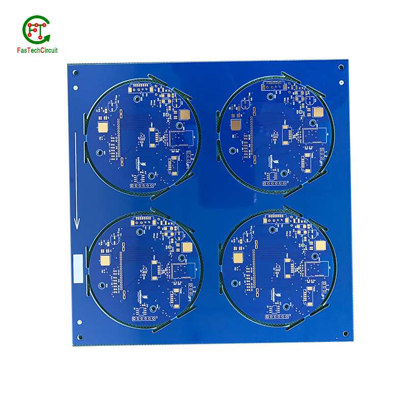
PCB assembly is a complex and intricate process that requires specialized knowledge and equipment. It involves the use of stencils, pick-and-place machines, reflow ovens, and inspection tools to accurately place and solder electronic components onto a circuit board. With the constantly evolving electronic industry, PCB assembly techniques are constantly improving to meet the demands for smaller, faster, and more efficient devices.
The materials used in PCB assembly are also important factors to consider. High-quality materials, such as FR-4 fiberglass, ensure the durability and reliability of the assembled PCB, especially for electronic devices that require long-term use.
PCB assembly is the process of assembling electronic components onto printed circuit boards (PCBs). It plays a critical role in the production of various electronic devices, from household appliances to advanced industrial equipment. However, as technology advances and the demand for higher quality products increases, there are often concerns and questions regarding the PCB assembly process. In this FQA (Frequently Asked Questions) section, we will address some commonly asked questions to provide a better understanding of PCB assembly.
2.What are the materials used in PCB assembly?
3.What is the most commonly used PCB material?
4.What are the 17 common manufacturing processing steps in PCB production?
5.What is PCB board components?
6.What is PCB assembly main?
7.What is the difference between PCB fabrication and PCB assembly?
8.What is disadvantage of PCB?
1.What is the difference between PCB and PCB assembly?
PCB (Printed Circuit Board) refers to the physical board that contains electronic components and their interconnections. It is the foundation of an electronic device and provides a platform for the components to be mounted and connected. PCB assembly, on the other hand, refers to the process of attaching electronic components to the PCB. This includes soldering or mounting the components onto the board, as well as testing and inspecting the finished product. In summary, PCB is the physical board while PCB assembly is the process of assembling electronic components onto the board.
2.What are the materials used in PCB assembly?
1. Printed Circuit Board (PCB): This is the base material on which the electronic components are mounted and connected. 2. Copper Foil: This is used to create the conductive traces on the PCB. 3. Solder Mask: This is a protective layer applied over the copper traces to prevent short circuits and corrosion. 4. Silkscreen: This is a layer of ink that is used to print component labels, reference designators, and other information on the PCB. 5. Solder Paste: This is a mixture of flux and solder particles used to attach the components to the PCB. 6. Electronic Components: These include resistors, capacitors, diodes, transistors, integrated circuits, and other electronic devices that make up the circuit. 7. Soldering Flux: This is a chemical used to clean and prepare the surfaces of the PCB and components for soldering. 8. Soldering Wire: This is used to create the electrical connections between the components and the PCB. 9. Adhesives: These are used to secure components to the PCB and to hold the PCB in place during the assembly process. 10. Thermal Interface Materials: These are used to improve heat transfer between components and the PCB. 11. Insulating Materials: These are used to prevent electrical contact between components and the PCB. 12. Cleaning Agents: These are used to remove flux residue and other contaminants from the PCB after assembly. 13. Packaging Materials: These are used to protect the finished PCB assembly during shipping and handling.
3.What is the most commonly used PCB material?
The most commonly used PCB material is FR-4 (Flame Retardant 4), which is a type of fiberglass epoxy laminate. It is widely used due to its high strength, good electrical insulation properties, and low cost.
4.What are the 17 common manufacturing processing steps in PCB production?
1. Design and Layout: The first step in PCB production is to create a design and layout of the circuit board using specialized software. 2. Material Selection: Once the design is finalized, the materials for the PCB are selected, including the substrate, copper foil, and solder mask. 3. Cutting: The substrate material is cut into the desired size and shape using a CNC machine or a laser cutter. 4. Drilling: Holes are drilled into the substrate for component placement and for creating electrical connections between layers. 5. Electroless Copper Deposition: A thin layer of copper is deposited on the substrate using a chemical process to create the conductive traces. 6. Imaging: A photosensitive layer called the resist is applied to the copper layer, and the PCB design is transferred onto it using a photomask and UV light. 7. Etching: The exposed copper is etched away using a chemical solution, leaving behind the desired circuit pattern. 8. Plating: A thin layer of copper is plated onto the remaining copper traces to increase their thickness and conductivity. 9. Solder Mask Application: A layer of solder mask is applied to the PCB to protect the copper traces and prevent short circuits. 10. Silkscreen Printing: The PCB is printed with component labels, logos, and other markings using a special ink called the silkscreen. 11. Surface Finish: A surface finish is applied to the exposed copper to protect it from oxidation and to improve solderability. 12. Electrical Testing: The PCB is tested for continuity and functionality using specialized equipment. 13. Component Placement: Electronic components such as resistors, capacitors, and ICs are placed on the PCB using automated pick-and-place machines. 14. Soldering: The components are soldered onto the PCB using a reflow oven or a wave soldering machine. 15. Inspection: The PCB is inspected for any defects or soldering errors using automated optical inspection (AOI) or manual inspection. 16. Final Testing: The assembled PCB is tested again to ensure that all components are functioning correctly. 17. Packaging and Shipping: The finished PCBs are packaged and shipped to the customer for use in electronic devices.
5.What is PCB board components?
PCB (Printed Circuit Board) board components are electronic components that are mounted on a PCB to create a functional electronic circuit. These components include resistors, capacitors, diodes, transistors, integrated circuits, connectors, and other electronic devices. They are soldered onto the PCB and connected through conductive traces to form a complete circuit. These components are essential for the proper functioning of electronic devices and are carefully selected and placed on the PCB according to the circuit design.

6.What is PCB assembly main?
PCB assembly, also known as printed circuit board assembly, is the process of attaching electronic components to a printed circuit board (PCB). This is a crucial step in the manufacturing of electronic devices, as it allows for the creation of a functional and operational circuit board. The main purpose of PCB assembly is to connect the electronic components to the PCB in a way that allows for the flow of electricity and the proper functioning of the device. This process involves various techniques such as soldering, surface mount technology, and through-hole technology. PCB assembly is a complex and precise process that requires specialized equipment and skilled technicians to ensure the quality and reliability of the final product.
7.What is the difference between PCB fabrication and PCB assembly?
PCB fabrication and PCB assembly are two distinct processes involved in the production of a printed circuit board (PCB). PCB fabrication, also known as PCB manufacturing, is the process of creating the bare PCB board by etching copper traces onto a non-conductive substrate. This involves several steps such as designing the PCB layout, printing the circuit onto the substrate, etching the copper traces, and drilling holes for components. The end result of this process is a bare PCB board with copper traces and holes for components. On the other hand, PCB assembly is the process of attaching electronic components onto the bare PCB board to create a functional electronic circuit. This involves placing the components onto the board, soldering them onto the copper traces, and testing the circuit for functionality. The end result of this process is a fully functional PCB that can be used in electronic devices. In summary, PCB fabrication is the process of creating the bare PCB board, while PCB assembly is the process of adding electronic components to the board to create a functional circuit. Both processes are essential in the production of a PCB and are often carried out by different companies or departments within a company.
8.What is disadvantage of PCB?
1. Fragility: PCBs are made of thin layers of materials that can be easily damaged or broken if not handled carefully. This makes them more fragile compared to other electronic components. 2. High Cost: The manufacturing process of PCBs involves several steps and the use of specialized equipment, which makes them more expensive compared to other alternatives. 3. Limited Flexibility: PCBs are rigid and cannot be easily bent or flexed, which limits their use in certain applications where flexibility is required. 4. Environmental Impact: The production of PCBs involves the use of chemicals and materials that can be harmful to the environment. Improper disposal of PCBs can also lead to pollution and health hazards. 5. Design Limitations: PCBs have a fixed design and cannot be easily modified or customized once they are manufactured. This can be a disadvantage for products that require frequent design changes. 6. Difficult Repair: In case of any damage or malfunction, repairing a PCB can be a complex and time-consuming process, requiring specialized skills and equipment. 7. Thermal Management: PCBs can generate a lot of heat, which can affect the performance and lifespan of electronic components. Proper thermal management techniques need to be implemented to prevent overheating. 8. Size Limitations: PCBs have a limited size and can only accommodate a certain number of components. This can be a disadvantage for complex electronic devices that require a large number of components. 9. Signal Interference: PCBs can be susceptible to electromagnetic interference, which can affect the performance of electronic components and lead to signal loss or distortion. 10. Lead-Free Regulations: Many countries have regulations that restrict the use of lead in electronic products, which can make it challenging to manufacture PCBs that meet these requirements.
RELATED NEWS


pcb board manufacturing How To Contact US
PCB from 1 to 30 layers, HDI, Heavy Copper, Rigid-flex board with "pcb board manufacturing One-Stop" service.