How do you calculate PCB assembly cost?
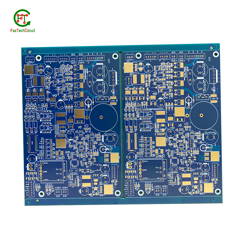
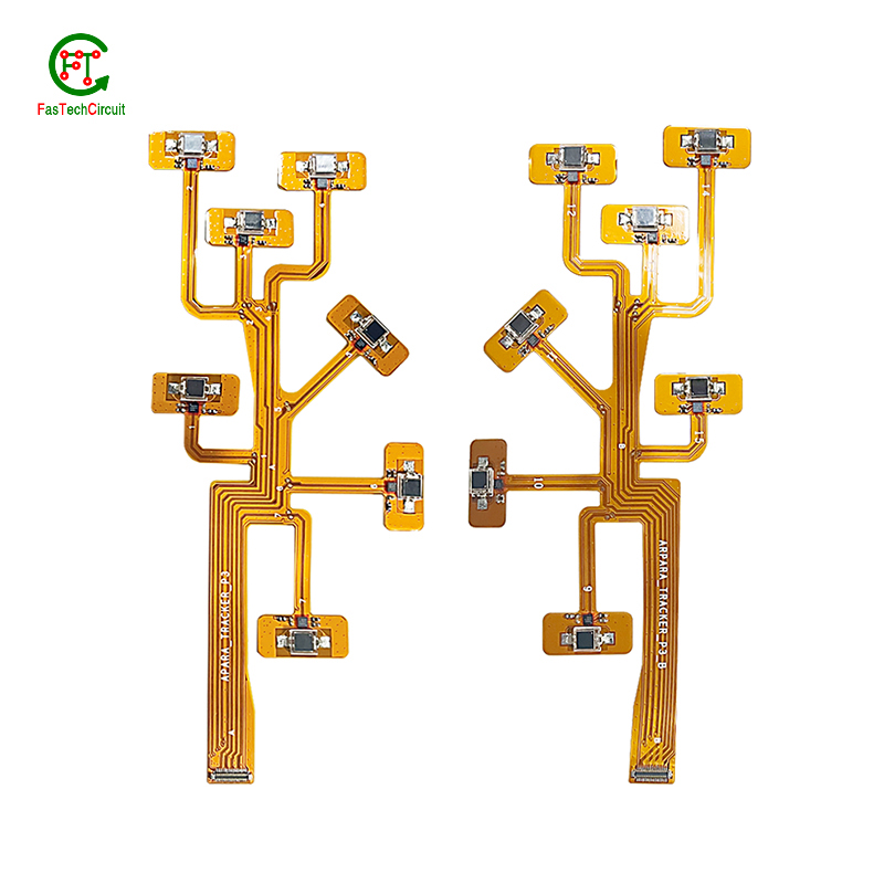
At its core, PCB assembly involves the placement and soldering of various electronic components onto a bare circuit board, typically made of fiberglass-reinforced epoxy or other composite materials. The electronic components are mounted onto the board using automated machines, with their connections being secured through soldering techniques.
The assembly process begins with the preparation of the bare circuit board, which is typically designed using computer-aided design (CAD) software. This ensures the accurate placement of components and their connections. The next step involves the insertion of electronic components onto the board, which is done using precision placement equipment. These components can range from simple resistors and capacitors to complex integrated circuits and microprocessors.
The actual assembly process is then performed using specialized machines that apply solder paste onto the board and place the components on the designated areas. The board is then heated in a controlled manner to melt the solder and create a strong connection between the components and the board. After the soldering process, the assembled PCB is thoroughly inspected for any defects, such as poor connections or missing components.
The benefits of PCB assembly are numerous. Not only does it provide a cost-effective and efficient method for producing electronic devices, but it also ensures consistency and accuracy in component placement, reducing the chances of errors and malfunctions. Additionally, PCB assembly allows for the creation of compact and lightweight electronic devices, making them ideal for various applications.
With the constant advancement of technology, PCB assembly has become a crucial part of our daily lives. It is used in a wide range of industries, including telecommunications, aerospace, automotive, and medical devices. The continuous development and improvement of PCB assembly techniques have also led to the creation of more sophisticated and complex electronic devices, such as smartphones, tablets, and wearable technology.

The demand for smaller and more powerful consumer electronics has increased the importance of efficient and effective PCB assembly. This process involves utilizing surface mount technology (SMT) and through-hole assembly methods to create compact and high-performance electronic products. With the use of automated equipment, the assembly process has become faster and more precise, enabling the production of a large number of products in a shorter period of time.
The materials used in PCB assembly are also important factors to consider. High-quality materials, such as FR-4 fiberglass, ensure the durability and reliability of the assembled PCB, especially for electronic devices that require long-term use.

PCB assembly is the process of assembling electronic components onto printed circuit boards (PCBs). It plays a critical role in the production of various electronic devices, from household appliances to advanced industrial equipment. However, as technology advances and the demand for higher quality products increases, there are often concerns and questions regarding the PCB assembly process. In this FQA (Frequently Asked Questions) section, we will address some commonly asked questions to provide a better understanding of PCB assembly.
2.What ISO is PCB manufacturing?
3.What technology is used in PCB?
4.What are the 7 steps of manufacturing?
5.How do you calculate PCB size?
6.What is the difference between PCB fabrication and PCB assembly?
1.What is the raw material of PCB assembly?
The raw material of PCB assembly includes: 1. Copper-clad laminate (CCL): This is the base material of the PCB, which is made of layers of fiberglass cloth and epoxy resin with a thin layer of copper on one or both sides. 2. Copper foil: This is the thin layer of copper that is laminated onto the CCL to create the conductive traces and pads on the PCB. 3. Solder mask: This is a layer of polymer resin that is applied over the copper traces to protect them from oxidation and to prevent solder from flowing onto unwanted areas during the assembly process. 4. Silk screen: This is a layer of ink that is applied over the solder mask to add labels, symbols, and other markings to the PCB. 5. Solder paste: This is a mixture of solder alloy particles and flux that is used to attach electronic components to the PCB. 6. Electronic components: These include resistors, capacitors, diodes, transistors, integrated circuits, and other electronic devices that are mounted onto the PCB. 7. Adhesives: These are used to bond components to the PCB and to hold the layers of the PCB together. 8. Flux: This is a chemical substance that is used to clean and prepare the surfaces of the PCB and components for soldering. 9. Solder: This is a metal alloy that is melted and used to create electrical connections between components and the PCB. 10. Lead-free materials: In some cases, lead-free materials may be used in the PCB assembly process to comply with environmental regulations. These materials include lead-free solder, lead-free components, and lead-free flux.
2.What ISO is PCB manufacturing?
The ISO standard for PCB manufacturing is ISO 9001:2015, which specifies requirements for a quality management system for organizations involved in the design, development, production, installation, and servicing of products. This standard ensures that PCB manufacturers have a consistent and effective quality management system in place to meet customer requirements and continuously improve their processes.
3.What technology is used in PCB?
1. Printed Circuit Board (PCB) Design Software: PCB design software is used to create the layout and design of the PCB. Popular software includes Altium Designer, Eagle PCB, and KiCad. 2. Computer-Aided Manufacturing (CAM) Software: CAM software is used to convert the PCB design into machine-readable instructions for the manufacturing process. 3. Computer-Aided Design (CAD) Software: CAD software is used to create 3D models of the PCB and its components, allowing for more accurate design and testing. 4. Computer Numerical Control (CNC) Machines: CNC machines are used to drill, cut, and etch the PCB according to the design specifications. 5. Surface Mount Technology (SMT): SMT is a method of placing and soldering electronic components directly onto the surface of the PCB, allowing for smaller and more compact designs. 6. Through-Hole Technology (THT): THT is a method of inserting electronic components through holes in the PCB and soldering them on the other side. 7. Soldering Equipment: Soldering equipment is used to melt and apply solder to the connections between components and the PCB. 8. Automated Optical Inspection (AOI) Systems: AOI systems use cameras and software to inspect the PCB for defects and ensure quality control during the manufacturing process. 9. X-Ray Inspection Systems: X-ray inspection systems are used to detect hidden defects in the PCB, such as faulty connections or missing components. 10. Automated Test Equipment (ATE): ATE is used to test the functionality of the PCB and its components, ensuring that they meet design specifications and function properly.
4.What are the 7 steps of manufacturing?
1. Conceptualization and Design: This is the first step in the manufacturing process where the idea for a product is developed and a design is created. 2. Material Selection: Once the design is finalized, the next step is to select the materials that will be used to make the product. 3. Prototyping: A prototype is created to test the design and make any necessary adjustments before moving on to mass production. 4. Tooling: Tooling refers to the creation of molds, dies, or other tools that will be used to manufacture the product. 5. Production: This is the stage where the actual manufacturing of the product takes place. It involves the use of machinery, assembly lines, and skilled labor to produce the product. 6. Quality Control: Quality control is an important step in the manufacturing process to ensure that the product meets the required standards and specifications. 7. Packaging and Distribution: Once the product is manufactured and passes quality control, it is packaged and prepared for distribution to retailers or customers. This step also includes logistics and transportation to get the product to its final destination.

5.How do you calculate PCB size?
To calculate the size of a PCB (printed circuit board), you will need to know the dimensions of the components that will be mounted on the board, as well as the spacing and placement of the components. You will also need to consider the size of the board itself, including any margins or borders. 1. Determine the dimensions of the components: Measure the length and width of each component that will be mounted on the PCB. This includes any integrated circuits, connectors, resistors, capacitors, etc. 2. Calculate the spacing between components: Determine the minimum spacing required between components to avoid interference or short circuits. This will depend on the size and type of components being used. 3. Add the spacing to the component dimensions: Add the spacing to the length and width of each component to determine the total size of each component on the PCB. 4. Determine the size of the board: Decide on the size of the PCB itself, including any margins or borders. This will depend on the size and number of components, as well as the desired layout and design. 5. Arrange the components on the board: Use a PCB design software or physical layout to arrange the components on the board. Make sure to leave enough space between components to avoid interference or short circuits. 6. Calculate the total size of the PCB: Add the dimensions of each component and the spacing between them to determine the total size of the PCB. 7. Consider additional factors: In addition to the components and spacing, you may also need to consider the size of the traces, vias, and other features on the PCB. These can also affect the overall size of the board. 8. Double-check your calculations: Make sure to double-check your calculations and measurements to ensure accuracy before ordering or manufacturing the PCB. Note: The size of the PCB may also be limited by the size of the production equipment or the manufacturer's capabilities. It is important to check with the manufacturer for any specific size limitations before finalizing the design.
6.What is the difference between PCB fabrication and PCB assembly?
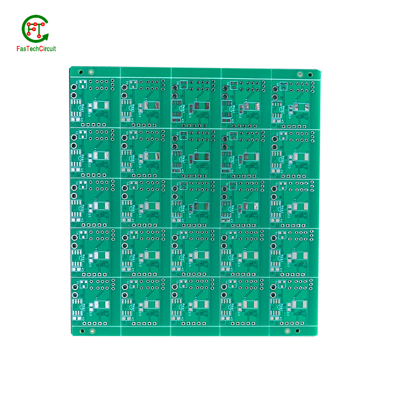
PCB fabrication and PCB assembly are two distinct processes involved in the production of a printed circuit board (PCB). PCB fabrication, also known as PCB manufacturing, is the process of creating the bare PCB board by etching copper traces onto a non-conductive substrate. This involves several steps such as designing the PCB layout, printing the circuit onto the substrate, etching the copper traces, and drilling holes for components. The end result of this process is a bare PCB board with copper traces and holes for components. On the other hand, PCB assembly is the process of attaching electronic components onto the bare PCB board to create a functional electronic circuit. This involves placing the components onto the board, soldering them onto the copper traces, and testing the circuit for functionality. The end result of this process is a fully functional PCB that can be used in electronic devices. In summary, PCB fabrication is the process of creating the bare PCB board, while PCB assembly is the process of adding electronic components to the board to create a functional circuit. Both processes are essential in the production of a PCB and are often carried out by different companies or departments within a company.
RELATED NEWS
pcb board manufacturing How To Contact US
PCB from 1 to 30 layers, HDI, Heavy Copper, Rigid-flex board with "pcb board manufacturing One-Stop" service.


