pcb manufacturing
Printed Circuit Board (PCB) is an important part of electronic equipment, which carries electronic components and realizes the connection and transmission of circuits. In the modern electronics industry, PCB manufacturing technology is becoming more and more mature. Not only can high-quality, high-density PCBs be manufactured, but also the application of PCBs in various fields can be realized through different materials and processes.
FasTechCircuit will give a detailed introduction to the PCB manufacturing process, including the basic structure, materials, manufacturing process, and future development trend of PCB technology.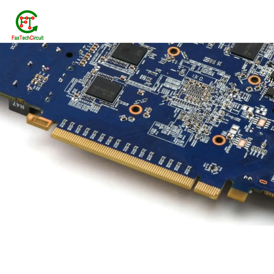
1. The basic structure of PCB
PCB usually consists of three parts: substrate, circuit layer and cover layer.
(1) Substrate
The substrate is the main body of the PCB, and it is usually made of materials with good electrical conductivity and high insulation properties, such as glass fiber, ceramics, polyimide, etc. The size, shape and thickness of the substrate depend on the use requirements of the electronic device, usually between 1-2mm.
(2) circuit layer
The circuit layer is the conductive layer on the PCB. It is made of copper foil, and the wiring and connection of the circuit can be realized by chemical processing, mechanical etching and other methods. The thickness of the circuit layer is usually between 35um-105um.
(3) Overlay
The cover layer is the protective layer on the PCB, which is made of insulating material, which can protect the circuit layer from mechanical damage, corrosion and oxidation. There are many types of covering layers, such as organic glue, epoxy resin, polyurethane, etc., among which organic glue is the most common.
2. PCB manufacturing materials
PCB manufacturing materials mainly include substrate materials, circuit layer materials, cover layer materials, and chemical reagents.
(1) Substrate material
The substrate material is the main body of the PCB, and its selection determines the performance and application range of the PCB. Commonly used substrate materials are glass fiber, ceramics, polyimide, polystyrene, etc.
(2) Circuit layer material
The circuit layer material is the conductive layer on the PCB, which is usually made of copper foil. The thickness and quality of copper foil determine the electrical conductivity and reliability of PCB.
(3)Overlay material
The cover layer material is the protective layer on the PCB, and its selection determines the protective performance and mechanical strength of the PCB. Commonly used cover materials include organic glue, epoxy resin, polyurethane, etc.
(4) chemical reagent
Chemical reagents are essential materials in the PCB manufacturing process, including etching solutions, film removal solutions, drilling fluids, etc. These chemical reagents can realize the manufacture and processing of PCB through different formulations and usage methods.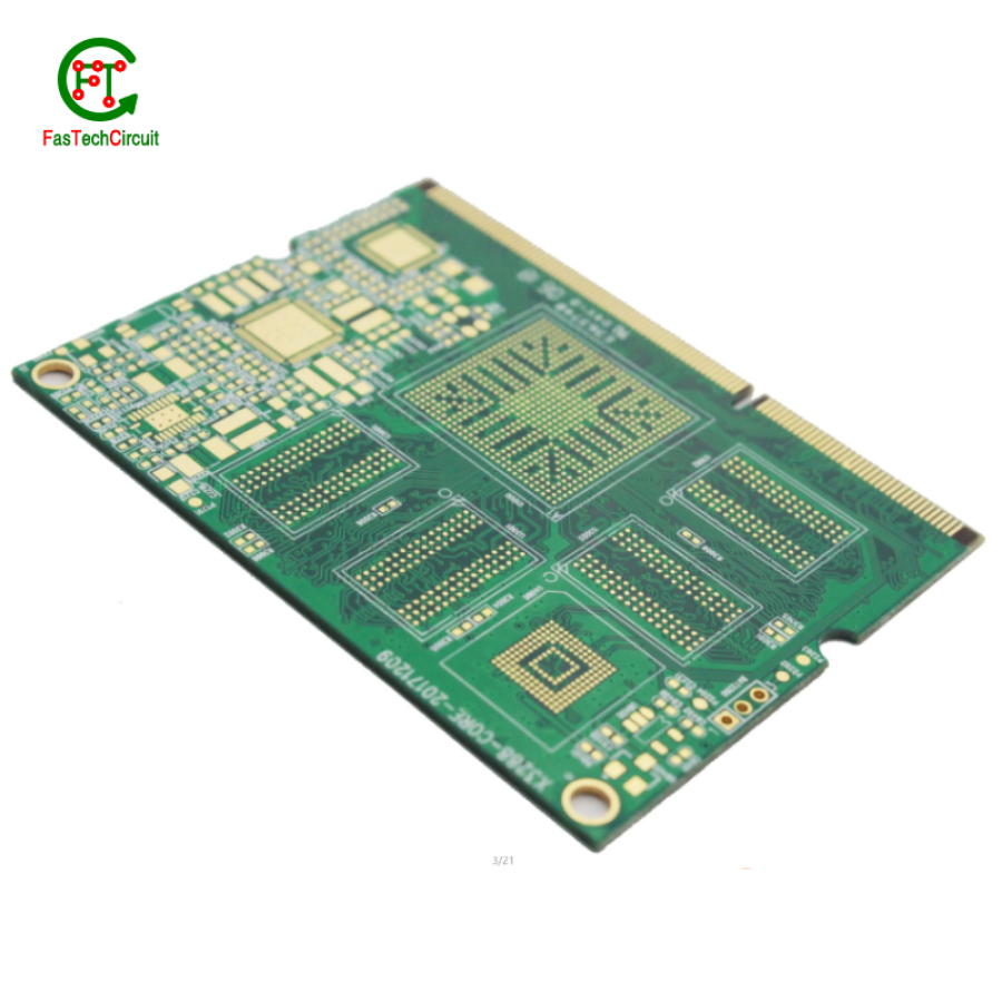
3. PCB manufacturing process
The manufacturing process of PCB includes multiple steps such as plate making, photo-painting, etching, drilling, metallization, covering layer, etc., each of which requires strict control and operation.
(1) board
Board making is the first step in PCB manufacturing, which usually consists of substrate materials and circuit layer materials. The process of plate making includes cutting, scraping, copper plating and other steps, which can be realized by mechanical or chemical methods.
(2) light painting
Photopainting is one of the key steps in PCB manufacturing, which forms circuit patterns on copper foil through photoresistive materials. The photopainting process includes multiple steps such as pattern design, imaging, and development, and requires the use of professional photopainting equipment and chemical reagents.
(3) etching
Etching is one of the key steps in PCB manufacturing. It chemically corrodes the copper foil that is not protected by the photoresistive material to form a circuit pattern. The etching process needs to control the concentration, temperature and time of chemical reagents to ensure the quality and precision of PCB.
(4) punch hole
Drilling is one of the important steps in PCB manufacturing. It drills holes into the PCB by mechanical or laser drilling machine to realize the installation and connection of circuit components.
(5) Metalization
Metallization is one of the key steps in PCB manufacturing, which chemically forms a metal layer on copper foil to enhance the electrical conductivity and reliability of PCB. The metallization process requires controlling the concentration, temperature and time of chemical reagents to ensure the uniformity and thickness of the metal layer.
(6) Overlay
Overlay is the last step in PCB manufacturing, it forms a protective layer on PCB by coating insulating material to protect PCB from mechanical damage, corrosion and oxidation. The type and thickness of the cover layer material need to be selected according to the use environment and requirements of the PCB.
(7) Fourth, the development trend of PCB technology
With the continuous development of electronic technology and the continuous expansion of application fields, PCB technology is also constantly innovating and improving. The future development trend of PCB technology mainly includes the following aspects.
(8) high density
High-density PCB is one of the important directions of PCB technology in the future. It realizes high-speed transmission and efficient operation of circuits by reducing the size of PCB and increasing the density of components.
(9) lead-free
Lead-free PCB is another important direction of PCB technology in the future. It achieves environmental protection and health requirements by using lead-free materials and processes.
(10) intelligent
Smart PCB is an emerging direction of PCB technology in the future. It realizes intelligent and autonomous control of circuits through embedded systems and wireless communication technologies.
(11) 3D printing technology
3D printing technology is one of the innovative directions of PCB technology in the future. It realizes the efficient manufacturing and application of PCB through rapid prototyping and customized production.
PCB is an important part of electronic equipment, and FasTechCircuit's manufacturing technology and application fields are constantly developing and innovating. The future development trend of PCB technology will be more diversified and intelligent, bringing more opportunities and challenges for the development and application of electronic equipment.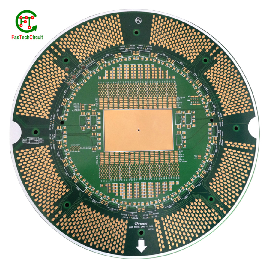
RELATED NEWS


pcb board manufacturing How To Contact US
PCB from 1 to 30 layers, HDI, Heavy Copper, Rigid-flex board with "pcb board manufacturing One-Stop" service.