How do you bake PCB before assembly?
At Fifth Metal Industrial Co.,LTD., we specialize in high-quality PCB assembly services, catering to a wide range of industries including automotive, aerospace, medical, and consumer electronics. Our advanced assembly facilities house state-of-the-art equipment and cutting-edge technology, allowing us to provide fast and accurate assembly of complex PCBs.
We offer a diverse range of assembly services including surface mount technology (SMT), through-hole technology (THT), and mixed technology. Our team of skilled technicians and engineers are well-versed in handling various types of components such as resistors, capacitors, integrated circuits, and many more. With their expertise and attention to detail, we ensure every component is precisely placed onto the PCB with the highest level of accuracy.
We understand the importance of quality and reliability in electronic products, which is why we implement strict quality control measures at every stage of the assembly process. Our PCB assembly services undergo rigorous testing, including functional and visual inspections, to ensure optimal performance and durability.
In addition to our assembly services, we also offer value-added services such as design for manufacturability (DFM) analysis, prototyping, and turnkey assembly. This allows for a streamlined production process and reduced lead times, ultimately providing our customers with a competitive edge in the market.
At Fifth Metal Industrial Co.,LTD., we pride ourselves on delivering cost-effective and efficient PCB assembly solutions without compromising on quality. We are committed to meeting our customers' specific requirements and providing them with impeccable service and support. Trust us to be your reliable partner for all your PCB assembly needs.

The materials used in PCB assembly are also important factors to consider. High-quality materials, such as FR-4 fiberglass, ensure the durability and reliability of the assembled PCB, especially for electronic devices that require long-term use.
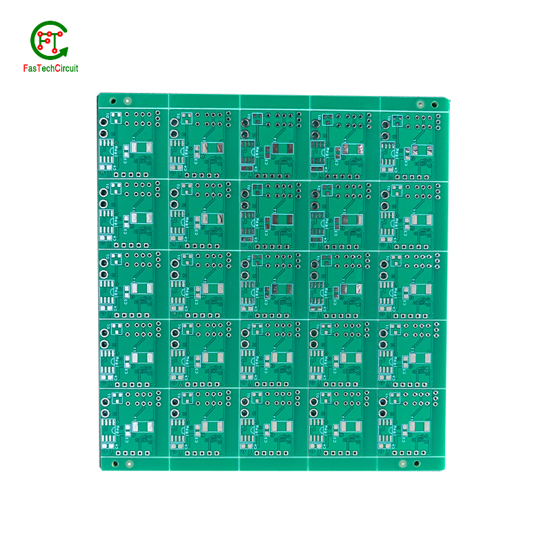
The assembly process begins with the design and layout of the PCB, which dictates the placement and orientation of components. Once the design is finalized, the components are placed using automated equipment or by hand. The PCB is then heated to melt the solder and create permanent connections between the components and the board.
PCB assembly is the process of assembling electronic components onto printed circuit boards (PCBs). It plays a critical role in the production of various electronic devices, from household appliances to advanced industrial equipment. However, as technology advances and the demand for higher quality products increases, there are often concerns and questions regarding the PCB assembly process. In this FQA (Frequently Asked Questions) section, we will address some commonly asked questions to provide a better understanding of PCB assembly.
2.What is PCB manufacturing?V
3.Why are PCBs so expensive?
4.Where are most PCBs made?
5.How do you calculate PCB assembly cost?
6.What is PCB lamination process?
7.What technology is used in PCB?
1.How is PCB thickness measured?
PCB thickness is typically measured in millimeters (mm) or mils (1 mil = 0.001 inches). It can be measured using a caliper or a thickness gauge specifically designed for PCBs. The measurement is taken from the top surface of the PCB to the bottom surface, including any copper layers, solder mask, and other coatings. The thickness can vary depending on the number of layers, materials used, and the manufacturing process.
2.What is PCB manufacturing?V
PCB (Printed Circuit Board) manufacturing is the process of producing printed circuit boards, which are used to mechanically support and electrically connect electronic components using conductive pathways, tracks, or signal traces etched from copper sheets laminated onto a non-conductive substrate. The manufacturing process involves several steps, including designing the PCB layout, printing the circuit pattern onto the substrate, etching the copper layers, drilling holes for component placement, and applying a protective solder mask and silkscreen. The final product is a functional PCB that can be used in various electronic devices. PCB manufacturing is a crucial part of the electronics industry and requires specialized equipment and expertise.
3.Why are PCBs so expensive?
1. Raw Materials: The materials used to make PCBs, such as copper, fiberglass, and epoxy resin, are expensive and can significantly contribute to the overall cost of the PCB. 2. Design Complexity: The more complex the design of the PCB, the more time and resources are required to manufacture it, leading to higher costs. 3. Manufacturing Process: The process of manufacturing PCBs involves multiple steps, including designing, printing, etching, drilling, and soldering, which require specialized equipment and skilled labor, making it a labor-intensive and time-consuming process. 4. Small Production Runs: PCBs are often produced in small quantities, which can drive up the cost per unit due to the lack of economies of scale. 5. Quality Control: PCBs need to undergo rigorous testing and quality control measures to ensure they meet the required standards, which can add to the overall cost. 6. Customization: Customized PCBs require additional time and resources to design and manufacture, making them more expensive than standard PCBs. 7. Environmental Regulations: PCBs are considered hazardous waste and must be disposed of properly, which can add to the cost of production. 8. Research and Development: The constant advancements in technology and the need for new and innovative PCB designs require significant investments in research and development, which can drive up the cost of PCBs. 9. Supply and Demand: The demand for PCBs is high, and the supply is limited, leading to higher prices. 10. Quality and Reliability: PCBs are critical components in electronic devices, and any defects or failures can have severe consequences. Therefore, manufacturers must invest in high-quality materials and processes, which can increase the cost of PCBs.
4.Where are most PCBs made?
Most PCBs (printed circuit boards) are made in China, followed by Taiwan, South Korea, Japan, and the United States. China is the largest producer of PCBs, accounting for over 50% of global production. This is due to the country's large electronics manufacturing industry and lower labor costs. Taiwan, South Korea, and Japan also have significant PCB production industries, while the United States has a smaller but still significant presence in the market.

5.How do you calculate PCB assembly cost?
The cost of PCB assembly can vary depending on several factors such as the complexity of the design, the number of components, the type of components, and the quantity of boards being assembled. To calculate the cost of PCB assembly, you can follow these steps: 1. Determine the cost of components: The first step is to determine the cost of all the components that will be used in the assembly. This includes the cost of the PCB, the cost of the electronic components, and any other materials that will be needed. 2. Calculate the labor cost: The labor cost will depend on the complexity of the design and the number of components that need to be soldered. You can estimate the labor cost by multiplying the number of hours it will take to assemble the PCB by the hourly rate of the assembly technician. 3. Add the cost of equipment and overhead: The cost of equipment and overhead, such as soldering equipment, inspection tools, and facility costs, should also be factored into the total cost. 4. Consider additional services: If you require additional services such as testing, programming, or conformal coating, you will need to add these costs to the total. 5. Calculate the total cost: Once you have determined all the individual costs, add them together to get the total cost of PCB assembly. It is important to note that the cost of PCB assembly can vary significantly depending on the manufacturer and the location. It is recommended to get quotes from multiple manufacturers to compare prices and choose the most cost-effective option.
6.What is PCB lamination process?
PCB lamination process is a manufacturing process used to bond multiple layers of a printed circuit board (PCB) together. This process involves the use of heat and pressure to fuse the layers of the PCB together, creating a single, solid board. The lamination process typically involves the following steps: 1. Preparation of the layers: The first step is to prepare the individual layers of the PCB. This includes cleaning, etching, and drilling the layers as per the design requirements. 2. Application of adhesive: A layer of adhesive material is applied to the surface of each layer. This adhesive helps to bond the layers together during the lamination process. 3. Layer alignment: The layers are then carefully aligned and stacked on top of each other, with the adhesive in between. 4. Lamination: The stacked layers are placed in a lamination press, which applies heat and pressure to fuse the layers together. The temperature and pressure are carefully controlled to ensure proper bonding without damaging the components on the PCB. 5. Cooling: After the lamination process, the PCB is cooled down to solidify the adhesive and create a strong bond between the layers. 6. Trimming and drilling: Once the PCB has cooled down, excess material is trimmed off the edges and holes are drilled to create the necessary connections between the layers. 7. Surface finishing: The final step is to apply a surface finish, such as solder mask or copper plating, to protect the PCB and provide a smooth surface for component placement. The lamination process is crucial in creating a strong and reliable PCB, as it ensures proper bonding between the layers and helps to maintain the integrity of the circuit.
7.What technology is used in PCB?
1. Printed Circuit Board (PCB) Design Software: PCB design software is used to create the layout and design of the PCB. Popular software includes Altium Designer, Eagle PCB, and KiCad. 2. Computer-Aided Manufacturing (CAM) Software: CAM software is used to convert the PCB design into machine-readable instructions for the manufacturing process. 3. Computer-Aided Design (CAD) Software: CAD software is used to create 3D models of the PCB and its components, allowing for more accurate design and testing. 4. Computer Numerical Control (CNC) Machines: CNC machines are used to drill, cut, and etch the PCB according to the design specifications. 5. Surface Mount Technology (SMT): SMT is a method of placing and soldering electronic components directly onto the surface of the PCB, allowing for smaller and more compact designs. 6. Through-Hole Technology (THT): THT is a method of inserting electronic components through holes in the PCB and soldering them on the other side. 7. Soldering Equipment: Soldering equipment is used to melt and apply solder to the connections between components and the PCB. 8. Automated Optical Inspection (AOI) Systems: AOI systems use cameras and software to inspect the PCB for defects and ensure quality control during the manufacturing process. 9. X-Ray Inspection Systems: X-ray inspection systems are used to detect hidden defects in the PCB, such as faulty connections or missing components. 10. Automated Test Equipment (ATE): ATE is used to test the functionality of the PCB and its components, ensuring that they meet design specifications and function properly.
RELATED NEWS


pcb board manufacturing How To Contact US
PCB from 1 to 30 layers, HDI, Heavy Copper, Rigid-flex board with "pcb board manufacturing One-Stop" service.