How are Multilayer PCBs different from Single-layer or Double-layer PCB, and why are they preferred for complex electronic designs?
Multilayer PCBs (Printed Circuit Boards) are electronic boards that consist of multiple layers of conductive copper traces and insulating material. They are different from single-layer or double-layer PCBs in terms of their construction, complexity, and capabilities. In this article, FasTechCircuit will explore the differences between Multilayer PCBs and Single-layer/Double-layer PCBs and why Multilayer PCBs are preferred for complex electronic designs.
Hot Tags: About FasTechCircuit ,More products
Differences between Multilayer PCBs and Single-layer/Double-layer PCB:
1. Construction:
Single-layer PCBs: As the name suggests, single-layer PCBs have only one layer of conductive traces on one side of the insulating substrate. All components and traces are placed on the same layer, making them relatively simple in construction.
Double-layer PCBs: Double-layer PCBs have two layers of conductive traces on both sides of the insulating substrate. Components and traces can be placed on both sides of the board, allowing for more complex circuit designs.
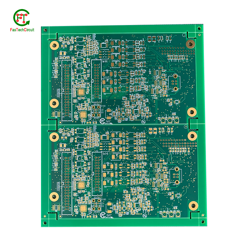
Multilayer PCBs: Multilayer PCBs consist of three or more layers of conductive traces separated by insulating layers. The number of layers can vary depending on the complexity of the design, ranging from four to dozens of layers.
2. Complexity and Capabilities:
Single-layer PCBs: Single-layer PCBs are limited in terms of complexity due to the single layer of traces available. They are typically used for simple circuits with fewer components and basic functionalities.
Double-layer PCBs: Double-layer PCBs allow for more complex designs by providing an additional layer of conductive traces. They can accommodate more components and provide better routing options for signal and power distribution.
Multilayer PCBs: Multilayer PCBs offer the highest level of complexity and capabilities due to the multiple layers of conductive traces. They are ideal for complex electronic designs that require a large number of components, high-speed signal transmission, and dense routing.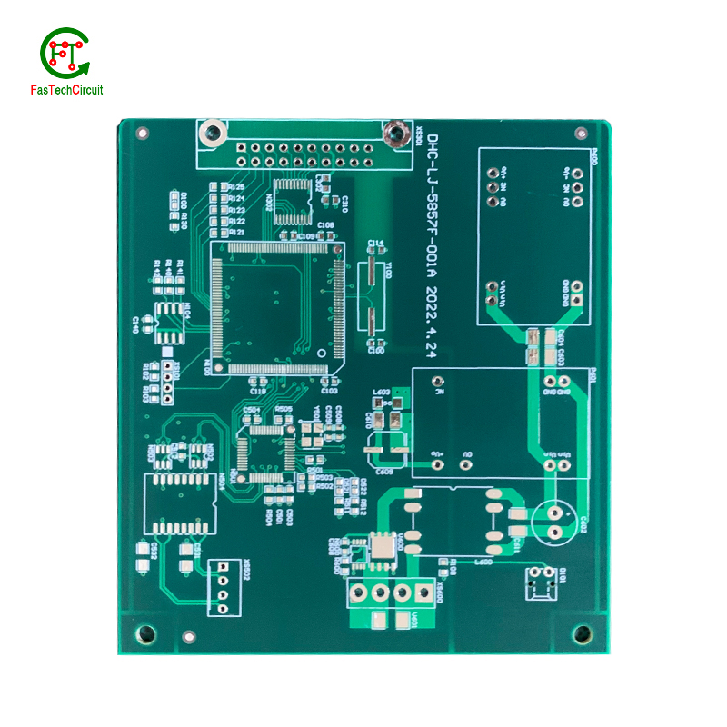
Advantages of Multilayer PCBs for Complex Electronic Designs:
3. High Density and Miniaturization: Multilayer PCBs allow for a high density of components and interconnections. With multiple layers of traces, designers have more space to place components and routes, enabling miniaturization and compact designs. This is particularly important for devices such as smartphones, tablets, and wearables where space is limited.
4. Improved Signal Integrity: Multilayer PCBs offer better signal integrity compared to single-layer or double-layer PCBs. The additional layers act as shielding, reducing electromagnetic interference (EMI) and crosstalk between traces. This helps to maintain signal integrity, reduce noise, and ensure reliable and high-quality performance of the electronic device.
5. Enhanced Power Distribution: Multilayer PCBs provide better power distribution capabilities compared to single-layer or double-layer PCBs. The additional layers allow for dedicated power planes, reducing power supply noise and voltage drops. This ensures stable and efficient power distribution to all components, especially for devices with high-power requirements.
6. Easier Routing and Design Flexibility: Multilayer PCBs offer more routing options and design flexibility. With multiple layers, designers can create complex and intricate routing patterns, optimizing signal paths and minimizing signal delays. This allows for efficient use of space and better organization of components, resulting in improved performance and manufacturability.
7. Reduced Electromagnetic Radiation: Multilayer PCBs help to reduce electromagnetic radiation, which is crucial for devices that need to comply with electromagnetic compatibility (EMC) regulations. The additional layers act as shields, containing electromagnetic emissions and reducing the impact on other components or nearby devices.
8. Enhanced Thermal Management: Multilayer PCBs enable better thermal management compared to single-layer or double-layer PCBs. The additional layers can be used for thermal vias and heat sinks, dissipating heat generated by components more effectively. This helps to prevent overheating and ensures the long-term reliability of the electronic device.
In conclusion, Multilayer PCBs differ from single-layer or double-layer PCBs in terms of their construction, complexity, and capabilities. Multilayer PCBs provide higher density, improved signal integrity, enhanced power distribution, easier routing, design flexibility, reduced electromagnetic radiation, and enhanced thermal management. These advantages make Multilayer PCBs the preferred choice for complex electronic designs that require high-performance, miniaturization, reliability, and compliance with industry standards.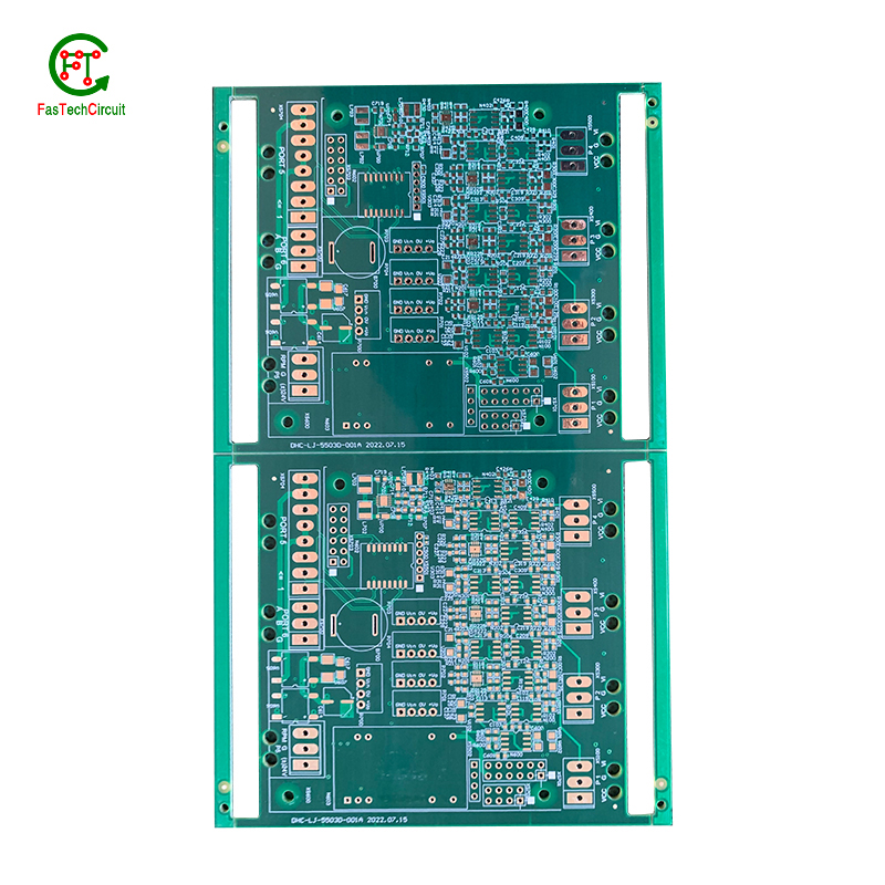
RELATED NEWS


pcb board manufacturing How To Contact US
PCB from 1 to 30 layers, HDI, Heavy Copper, Rigid-flex board with "pcb board manufacturing One-Stop" service.