5730 led pcb board
| Base Material | FR-4/CEM-1/CEM-3/Polyimild/PTFE/Rogers |
| Board Thickness | 0.1-8mm |
| Model Number | Custom PCB & PCB Assembly |
| Type | Aluminum PCB |
| Brand Name | FC |
| Copper Thickness | 0.5-2mil(12-49um) |
| Min. Hole Size | 0.1mm(4mil)for HDI / 0.15mm(6mil) |
| Min. Line Width | 0.075mm/0.075mm(3mil/3mil) |
| Min. Line Spacing | 0.003'' |
| Surface Finishing | HASL/OSP/Ag/ENIG/ENEPIG/Immersion silver/Tin |
| Board Size | Custom |
| Model Number | Customized |
| Base Material | FR4 Aluminum CEM-1 94V0 |
| Surface Finishing | HASLENIG OSP |
| Number of layer | 1-13layer |
| Other service | Components purchasing and assem |
| ly Solder mask | White Black Green Blue,Red,etc. |
| Dsign service | Available |
| Testing | Function testing |
| Certificate | RoHS, ISO/TS16949, ISO9001 |
| Name | High Quality led light aluminum pcb printed circuit board |
| Packaging Details | Vaccum package and standard carton outside High Quality led light aluminum pcb printed circuit board |
| Supply Ability | 43702 Square Meter/Square Meters per Month |
| Quantity (pieces) | > 17190 |
| Lead time (days) | 14 |
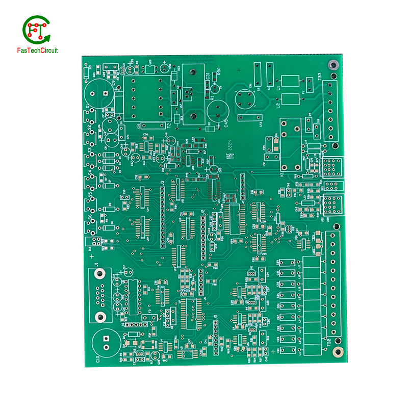
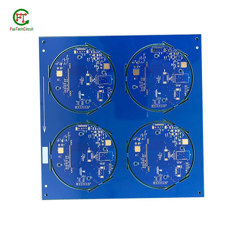
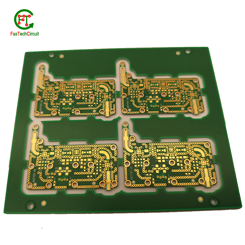
5730 led pcb board bearings FAQs Guide Welcome to our state-of-the-art PCB (Printed Circuit Board) products. We are proud to offer a comprehensive range of high-quality and versatile PCB solutions to meet the constantly evolving needs of the modern electronics industry.Our PCBs are expertly designed and manufactured using the latest technology and advanced techniques, ensuring reliability, durability, and exceptional performance for a wide range of applications. We understand the importance of precision and attention to detail in the production of PCBs and we are committed to meeting stringent quality standards.
2.How are signal traces routed on a 5730 led pcb board?
3.How are through-hole components soldered onto a 5730 led pcb board?
4.How does a 5730 led pcb board work?
5.What is the difference between a copper pour and a trace on a 5730 led pcb board?
6.Can 5730 led pcb boards be used in high voltage applications?
7.How are high-frequency signals handled on a 5730 led pcb board?
8.How are 5730 led pcb boards manufactured?
9.What is the typical lifespan of a 5730 led pcb board?
10.What is the role of a data sheet in 5730 led pcb board design?
11.How are power and ground planes connected on a 5730 led pcb board?
12.What is the maximum size of a 5730 led pcb board?
13.How are signal integrity issues addressed in 5730 led pcb board design?
14.What type of material is used for the silkscreen on a 5730 led pcb board?
1.What is the minimum size of a through-hole component that can be used on a 5730 led pcb board?
We continue to invest in research and development and continue to launch innovative products.
The minimum size of a through-hole component that can be used on a PCB depends on the capabilities of the PCB manufacturer and the design requirements of the circuit. Generally, the minimum size for a through-hole component is around 0.2mm in diameter, but some manufacturers may be able to produce smaller sizes. It is important to consult with the manufacturer and consider the design requirements to determine the appropriate size for a through-hole component on a PCB.
2.How are signal traces routed on a 5730 led pcb board?
Signal traces are an essential element of a PCB, responsible for carrying electronic signals between components and ensuring proper communication and functionality of the circuit. To route these traces, designers use specialized software to determine the most efficient and optimal path for each signal, taking into account factors such as signal integrity, trace length, and potential interference. This process involves careful planning, as well as techniques such as vias, ground and power planes, and differential pairs to minimize noise and maintain signal integrity.
3.How are through-hole components soldered onto a 5730 led pcb board?
Through-hole components are soldered onto a printed circuit board (PCB) using a process called wave soldering. First, the PCB is fitted with all the necessary through-hole components, such as resistors, capacitors, and diodes. Then, the board is passed over a wave of molten solder, which flows through the holes in the PCB and creates a secure connection between the component and the board. The excess solder is removed and the board is inspected to ensure all components are properly soldered. This method of soldering provides a strong and reliable connection for through-hole components, making it a popular choice for electronic assembly.
4.How does a 5730 led pcb board work?
We maintain a stable growth through reasonable capital operations, focus on industry development trends and cutting -edge technologies, and focus on product quality and safety performance.
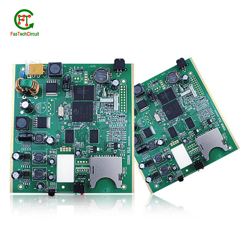
A PCB (Printed Circuit Board) is a thin board made of non-conductive material, such as fiberglass or plastic, with conductive pathways etched or printed onto its surface. These pathways, also known as traces, are used to connect electronic components on the board, such as resistors, capacitors, and integrated circuits.
The PCB works by providing a platform for the components to be mounted and connected in a specific circuit configuration. The traces on the board act as wires, allowing electricity to flow between the components and creating a complete circuit.
The process of creating a PCB involves several steps, including designing the circuit layout, printing or etching the traces onto the board, and attaching the components using soldering techniques. Once the components are attached, the board is tested to ensure that all connections are correct and functioning properly.
When a PCB is connected to a power source, electricity flows through the traces, powering the components and allowing them to perform their intended functions. The traces also act as a pathway for signals to travel between components, allowing for communication and data transfer within the circuit.
PCBs are used in a wide range of electronic devices, from simple household appliances to complex computer systems. They provide a compact and efficient way to connect and control electronic components, making them an essential part of modern technology.
5.What is the difference between a copper pour and a trace on a 5730 led pcb board?
We adhere to the principle of quality first and have a complete production quality management system and quality inspection process.
A copper pour and a trace are two common electronic components that are found on a printed circuit board (PCB). A copper pour is a large area of copper that is used to connect multiple components or ground signals together on a PCB. This creates a solid and low resistance pathway for signals to flow. On the other hand, a trace is a thin line of copper used to connect individual components on a PCB. It carries a specific signal from one component to another. Unlike a copper pour, a trace can be designed to carry a specific current and have a specific width to meet the requirements of the circuit.
6.Can 5730 led pcb boards be used in high voltage applications?
We have advantages in marketing and channel expansion. Suppliers have established good cooperative relations, continuously improved workflows, improved efficiency and productivity, and provided customers with high -quality products and services.
Yes, PCBs (printed circuit boards) can be used in high voltage applications. However, the design and construction of the PCB must be carefully considered to ensure it can withstand the high voltage without causing damage or malfunction. This may include using specialized materials, increasing the spacing between components, and implementing proper insulation and grounding techniques. It is important to consult with a qualified engineer or designer when using PCBs in high voltage applications to ensure safety and reliability.
7.How are high-frequency signals handled on a 5730 led pcb board?
High-frequency signals are typically handled with great care and precision on a PCB to ensure optimal performance. This involves using high-quality materials, such as high-speed laminates and low-loss dielectrics, to minimize signal loss and interference. Additionally, designers must carefully consider the trace routing and placement of components on the PCB to minimize signal reflections and keep the signal path as short and direct as possible. Specialized techniques, like controlled impedance and shielding, may also be used to further improve signal integrity.
8.How are 5730 led pcb boards manufactured?
We have the leading technology and innovation capabilities, and attach importance to employee training and development, and provide promotion opportunities.
PCB are manufactured through a series of steps starting with designing the circuit layout. Once the design is finalized, the layout is printed on a special type of paper known as the “artwork”. This artwork is then transferred onto a copper-coated laminate board through a process called etching. The excess copper is removed, leaving behind the desired circuit pattern. The board is then drilled to create holes for components to be inserted. The next step involves adding a thin layer of solder mask to protect the circuit and adding a thin layer of copper to create traces. Finally, the components are added using a specialized machine, and the board goes through a series of tests to ensure proper functionality. Once the tests are passed, the board is cut and separated into individual PCBs for use in various electronic devices.
9.What is the typical lifespan of a 5730 led pcb board?
5730 led pcb board is not a product only, but also can help you comes to money-making.
The typical lifespan of a PCB (printed circuit board) can vary greatly depending on various factors such as the quality of materials used, environmental conditions, and usage. In general, a well-designed and properly manufactured PCB can last for 10-20 years or more. However, some PCBs may fail prematurely due to factors such as corrosion, thermal stress, or mechanical damage. Regular maintenance and proper handling can also extend the lifespan of a PCB.
10.What is the role of a data sheet in 5730 led pcb board design?
A data sheet is an essential tool for PCB design, providing vital information and specifications for all of the components used in the design process. It contains detailed technical data, such as dimensions, electrical ratings, and performance characteristics, that allow designers to make informed decisions when selecting and placing components on a PCB. By referencing the data sheet, designers can ensure that each component is properly integrated into the overall design, following any necessary guidelines or restrictions. Additionally, data sheets also provide necessary information for the layout and routing of traces on the PCB, ensuring that the design can meet required performance specifications.
11.How are power and ground planes connected on a 5730 led pcb board?
Power and ground planes are typically connected on a PCB through vias, which are small holes drilled through the layers of the PCB. These vias are filled with conductive material, such as copper, and allow for the flow of current between the power and ground planes. The vias are strategically placed throughout the PCB to ensure a low impedance connection between the power and ground planes. Additionally, traces or copper pours can also be used to connect the power and ground planes on different layers of the PCB.
12.What is the maximum size of a 5730 led pcb board?
We pay attention to the introduction and training of talents, scientifically regulate the management system, and focus on cultural construction and team cohesion.
The maximum size of a PCB (printed circuit board) can vary depending on the manufacturer and theircapabilities. However, the industry standard maximum size for a single PCB panel is typically around 18 inches by 24 inches (457 mm by 610 mm). Larger PCBs can be created by combining multiple panels together. Some manufacturers may also have the capability to create custom-sized PCBs that exceed the industry standard maximum size.
13.How are signal integrity issues addressed in 5730 led pcb board design?
We focus on our customers' needs and strive to meet their expectations, so we take this very seriously.
Signal integrity issues are a common concern in PCB design, as they can greatly affect the performance and reliability of electronic systems. These issues arise from high-speed signal transmissions on the board, which can result in degraded signals, data errors, and even system failures. In order to address these issues, PCB designers must consider various factors such as layout, routing, and component placement to ensure proper signal integrity. This involves implementing signal protection measures such as controlled impedance routing, signal shielding, and minimizing signal crosstalk. Additionally, designers may use simulation and analysis tools to identify and resolve any potential signal integrity problems before the PCB goes into production. By carefully addressing signal integrity issues in the design phase, PCBs can achieve optimal performance and functionality.
14.What type of material is used for the silkscreen on a 5730 led pcb board?
We have a wide range of 5730 led pcb board customer groups and establishes long -term cooperative relationships with partners. The countries we provide services include .
The material used for the silkscreen on a PCB is typically a white or black ink made of epoxy or acrylic. It is applied using a screen printing process and is cured at high temperatures to ensure durability and resistance to chemicals and solvents.
RELATED PRODUCTS & SERVICE
pcb board manufacturing How To Contact US
PCB from 1 to 30 layers, HDI, Heavy Copper, Rigid-flex board with "pcb board manufacturing One-Stop" service.

