2 layer pcb board
We built a factory in Shenzhen; our factory's designed production capacity can reach up to 25,000 square meters per month. We purchase and assemble the most advanced production equipment from China, Germany, Japan to ensure the best quality of our PCBs; We have ISO-9001 quality system certification and ISO-14001 environmental system certification. All of our PCBs are UL certified. Fast response, strict quality control, best service, strong technical support and effective improvement enable HFasTechCircuit to export our PCB products to the global market, which are widely used in the telecommunications industry, automobile industry, computer, home appliance industry, and Large LED equipment; we can provide one-stop OEM service, price advantage, and fast delivery! Our products are very popular in Yemen,Nigeria,Chad, the United States and Japan. Won high praise from customers.
| Number of Layers | 4 layer |
| Base Material | gold sinking |
| Board Thickness | 2.5MM |
| Board Size | 280M*599MM |
| Model Number | 4 layer pcb |
| Type | pcb |
| Place of Origin | Original |
| Brand Name | Original |
| Copper Thickness | 3OZ |
| Min. Hole Size | custom made |
| Min. Line Width | custom made |
| Min. Line Spacing | custom made |
| Surface Finishing | custom made |
| Impedance control | +/- 7% |
| Warpage | less than 1% |
| Packaging Details | New and Original, factory sealed packing, it will be pack in one of these packing type: Tube, Tray, Tape and Reel, Tape and Box, Bulk packing, Bag and etc. Please kindly contact us for more details. |
| Supply Ability | 5434 Piece/Pieces per Week |
| Quantity (pieces) | > 14601 |
| Lead time (days) | 12 |
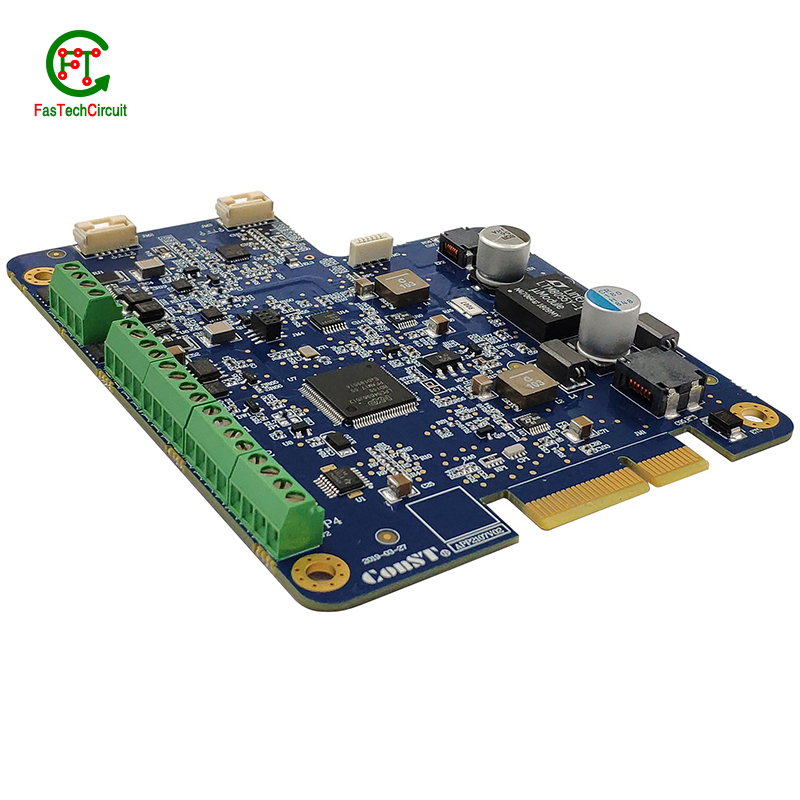
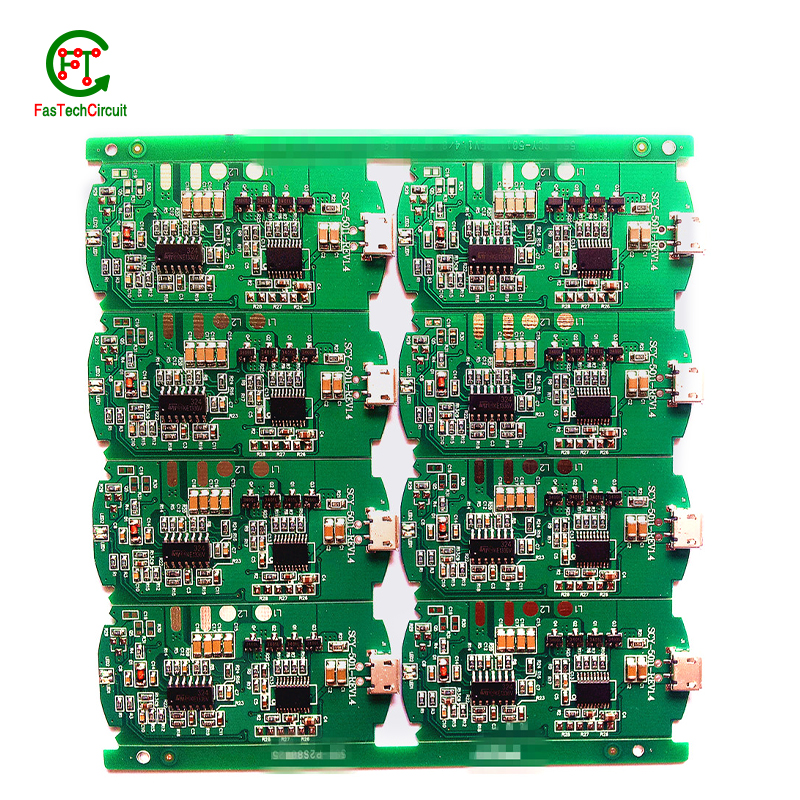
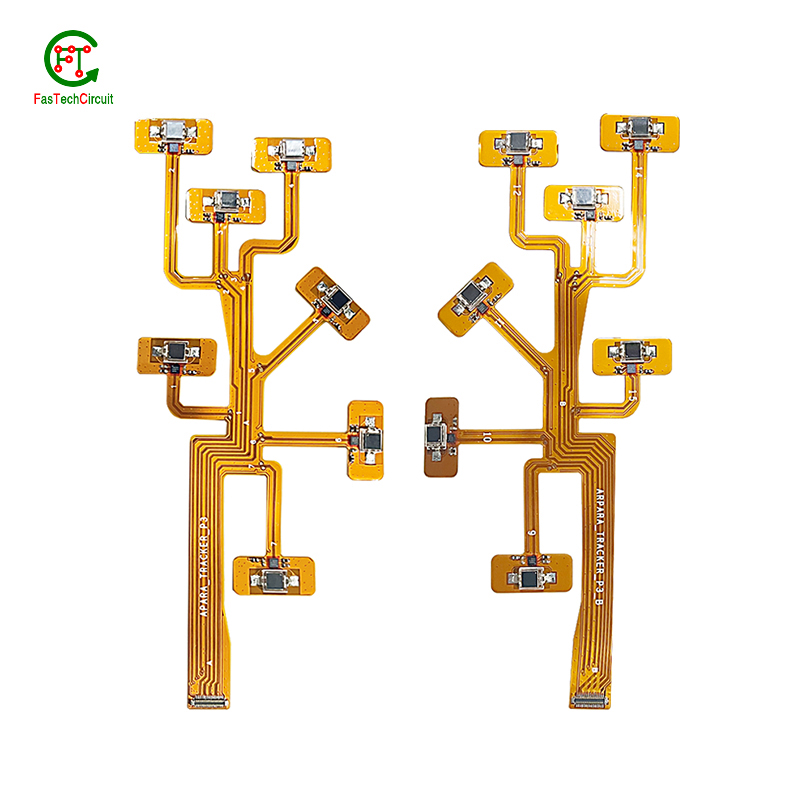
2 layer pcb board bearings FAQs Guide Welcome to our state-of-the-art PCB (Printed Circuit Board) products. We are proud to offer a comprehensive range of high-quality and versatile PCB solutions to meet the constantly evolving needs of the modern electronics industry.Our PCBs are expertly designed and manufactured using the latest technology and advanced techniques, ensuring reliability, durability, and exceptional performance for a wide range of applications. We understand the importance of precision and attention to detail in the production of PCBs and we are committed to meeting stringent quality standards.
2.What is the role of vias on a 2 layer pcb board?
3.What is the purpose of a ground plane on a 2 layer pcb board?
4.What is the typical lifespan of a 2 layer pcb board?
5.How is a 2 layer pcb board tested for functionality?
6.How are 2 layer pcb board used in medical devices?
7.What is the difference between single-sided, double-sided, and multi-layer 2 layer pcb board?
8.What is a 2 layer pcb board?
9.What does 2 layer pcb board stand for?
10.How are signal traces routed on a 2 layer pcb board?
11.How are high-speed/high-frequency 2 layer pcb board tested and validated?
12.What is the function of a decoupling capacitor on a 2 layer pcb board?
13.What is the difference between an analog and a digital signal on a 2 layer pcb board?
1.What are the benefits of using surface mount technology (SMT) for 2 layer pcb board?
We focus on innovation and continuous improvement to maintain a competitive advantage.
Surface mount technology (SMT) is a popular method for assembling printed circuit boards (PCBs) that offers numerous benefits over traditional through-hole components. Firstly, SMT components are smaller and more compact, allowing for greater PCB density and reducing the overall size of the board. This makes SMT ideal for increasingly miniaturized electronics, such as smartphones and wearables. Additionally, SMT components are typically cheaper and easier to manufacture, leading to cost savings in both materials and labor. SMT also allows for automated assembly, resulting in faster and more efficient production processes. Furthermore, the smaller size of SMT components leads to improved electrical performance due to decreased parasitic effects and shorter signal paths. This makes SMT ideal for high-frequency applications.
2.What is the role of vias on a 2 layer pcb board?
Our company has many years of 2 layer pcb board experience and expertise.
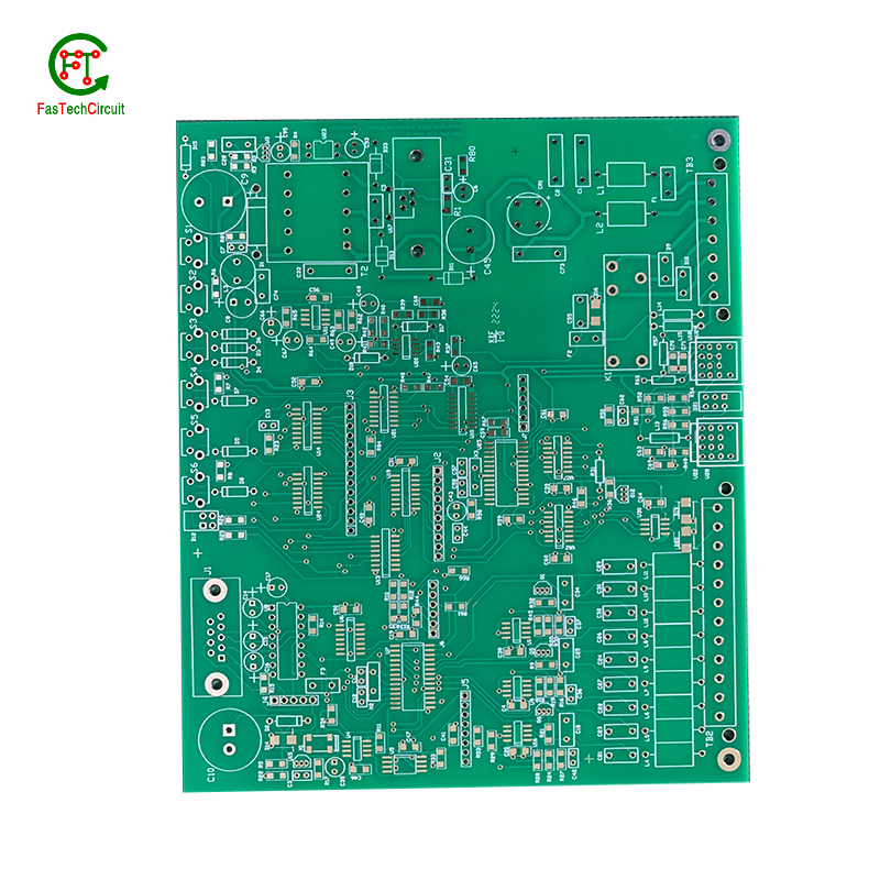
Vias play a crucial role in connecting different layers of a printed circuit board (PCB). These small, plated holes act as conductive paths, allowing signals and power to pass through the board and reach various components. Vias are also essential for routing traces from one layer to another, optimizing the layout and reducing the size and complexity of the board. Additionally, vias provide structural support and improve thermal management by facilitating heat dissipation.
3.What is the purpose of a ground plane on a 2 layer pcb board?
I have a comprehensive after -sales service system, which can pay attention to market trends in time and adjust our strategy in a timely manner.
A decoupling capacitor is an essential component on a PCB (Printed Circuit Board) which is used to reduce or eliminate high frequency noise between different components. It acts as a buffer between the power supply and other circuit components, by storing electrical charge and then releasing it when there is a sudden change in the supply voltage. This helps to stabilize the power supply, providing a steady and noise-free flow of electricity to the circuit. Furthermore, decoupling capacitors also help to filter out any unwanted signals that may cause interference or disruptions in the proper functioning of the circuit.
4.What is the typical lifespan of a 2 layer pcb board?
2 layer pcb board is not a product only, but also can help you comes to money-making.
The typical lifespan of a PCB (printed circuit board) can vary greatly depending on various factors such as the quality of materials used, environmental conditions, and usage. In general, a well-designed and properly manufactured PCB can last for 10-20 years or more. However, some PCBs may fail prematurely due to factors such as corrosion, thermal stress, or mechanical damage. Regular maintenance and proper handling can also extend the lifespan of a PCB.
5.How is a 2 layer pcb board tested for functionality?
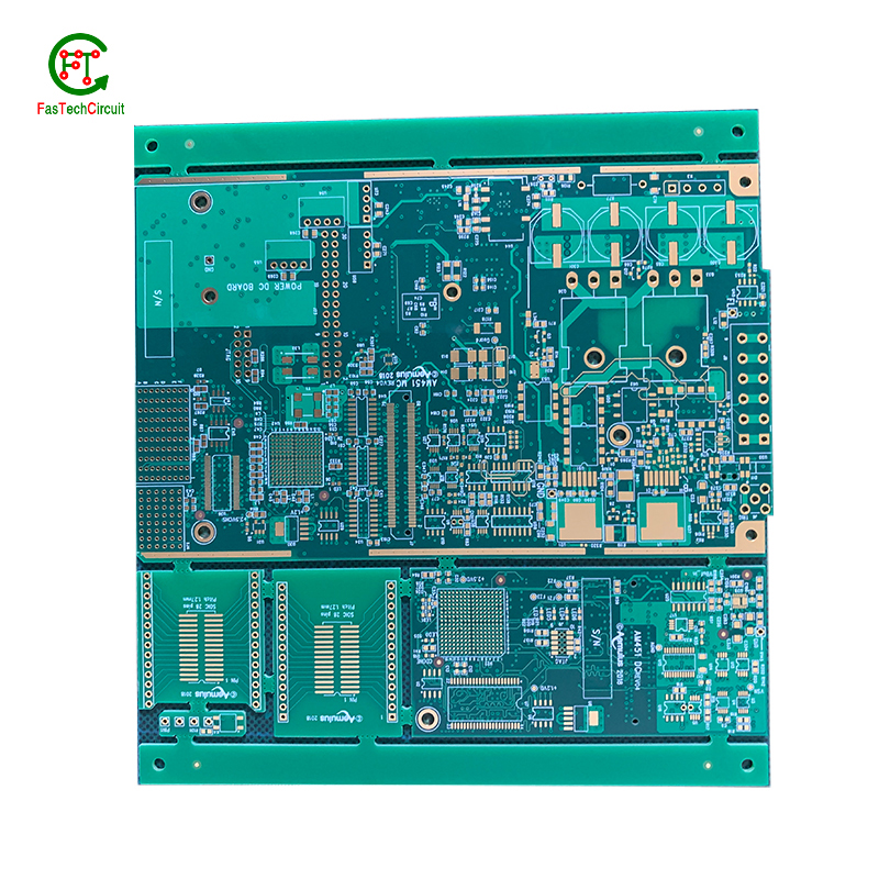
A PCB, or Printed Circuit Board, is tested for functionality to ensure that all components and connections on the board are working correctly. This is important in order to detect any potential manufacturing or design defects that could compromise the board's performance. To test a PCB, a range of diagnostic tools and techniques are used including visual inspection, automated testing software, and specialized equipment such as oscilloscopes and multimeters. Experienced technicians also use their knowledge and expertise to troubleshoot and identify any issues with the board. Through this rigorous testing process, any faults or failures are identified and resolved before the PCB is released for production, ensuring that it meets the desired functionality and performance standards.
6.How are 2 layer pcb board used in medical devices?
Printed Circuit Boards (PCBs) are essential components used in a wide range of medical devices, playing a crucial role in both diagnostic and treatment equipment. These devices require reliable and precise circuitry to accurately collect and process data, deliver therapies, and regulate medical procedures. PCBs are used in equipment such as MRI machines, pacemakers, defibrillators, and monitors, where their small size and high density make them ideal for compact and portable designs. In addition, PCBs are also used in medical implants, enabling a safe and secure connection between the device and the body. With their advanced technology, PCBs continue to be an integral part of the medical industry, ensuring the effectiveness and success of various medical procedures and treatments.
7.What is the difference between single-sided, double-sided, and multi-layer 2 layer pcb board?
We have established a good reputation and reliable partnerships within the 2 layer pcb board industry.
Single-sided PCB (Printed Circuit Board) is a type of PCB that has components and traces on only one side of the board. The other side is usually used for soldering and mounting the board onto a larger circuit.
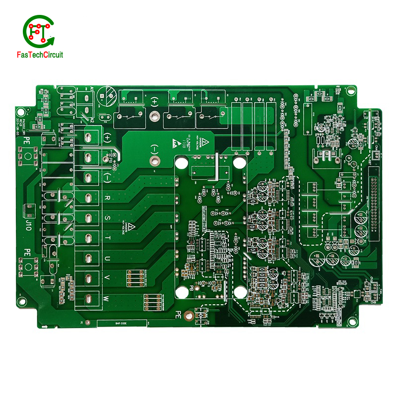
Double-sided PCB is a type of PCB that has components and traces on both sides of the board. The traces on both sides are connected through vias, which are small holes drilled through the board and plated with metal to create an electrical connection.
Multi-layer PCB is a type of PCB that has multiple layers of conductive material and insulating material sandwiched together. The layers are connected through vias, allowing for more complex and compact circuit designs. Multi-layer PCBs are used in more advanced and high-performance electronic devices.
8.What is a 2 layer pcb board?
We pay attention to user experience and product quality, and provide the best product quality and lowest production cost for cooperative customers.
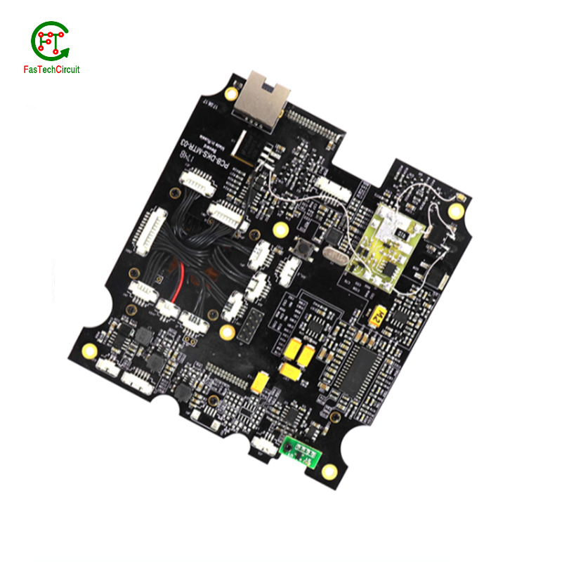
A PCB (Printed Circuit Board) is a flat board made of non-conductive material, such as fiberglass, with conductive pathways etched or printed onto it. It is used to mechanically support and electrically connect electronic components using conductive tracks, pads, and other features etched from copper sheets laminated onto a non-conductive substrate. PCBs are commonly used in electronic devices such as computers, smartphones, and televisions to provide a platform for the components to be mounted and connected together. They are also used in a variety of other applications, including automotive, aerospace, and medical devices.
9.What does 2 layer pcb board stand for?
We attach importance to the innovation ability and team spirit of employees, have advanced R & D facilities and laboratories, and have a good quality management system.
PCB stands for Printed Circuit Board.
10.How are signal traces routed on a 2 layer pcb board?
Signal traces are an essential element of a PCB, responsible for carrying electronic signals between components and ensuring proper communication and functionality of the circuit. To route these traces, designers use specialized software to determine the most efficient and optimal path for each signal, taking into account factors such as signal integrity, trace length, and potential interference. This process involves careful planning, as well as techniques such as vias, ground and power planes, and differential pairs to minimize noise and maintain signal integrity.
11.How are high-speed/high-frequency 2 layer pcb board tested and validated?
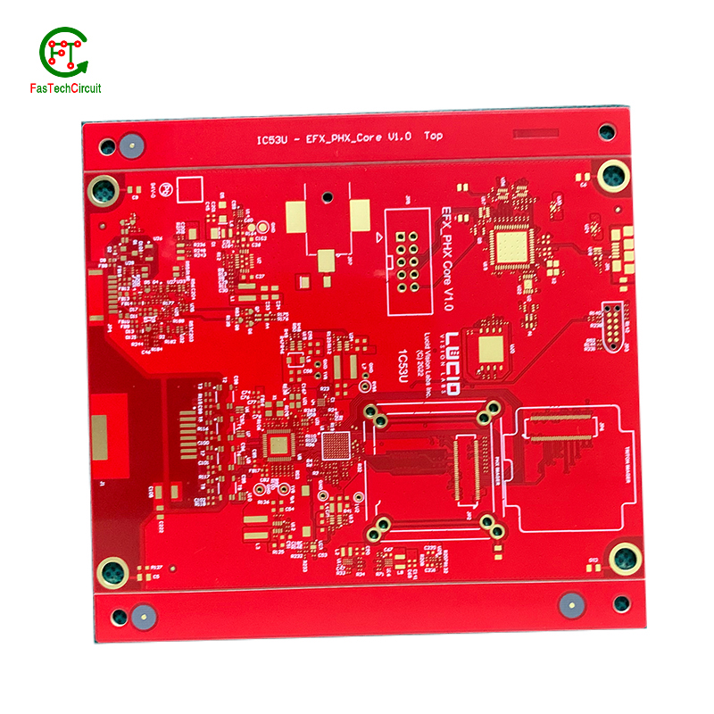
Testing and validation are essential steps in the production process of high-speed and high-frequency printed circuit boards (PCBs). These specialized types of PCBs are used in a wide range of industries, including telecommunications, aerospace, and automotive, and require precision and reliability in their performance.
The testing and validation process for high-speed/high-frequency PCBs involves several steps to ensure that the final product meets the required specifications. This starts with design simulation and analysis using specialized software to verify the layout and electrical characteristics of the PCB.
Once the design is confirmed, prototype PCBs are manufactured and subjected to various tests, including signal integrity and power integrity tests. These tests evaluate the electrical performance of the PCB, such as its ability to transmit signals at high speeds and maintain signal integrity.
In addition to electrical tests, environmental and mechanical tests are also performed to assess the durability and reliability of the PCB under different conditions, such as temperature changes and mechanical stress.
The final step in the testing and validation process is the inspection and analysis of the tested PCBs. This involves a detailed review of the test results and any necessary modifications to meet the required specifications.
12.What is the function of a decoupling capacitor on a 2 layer pcb board?
We have rich industry experience and professional knowledge, and have strong competitiveness in the market.
A decoupling capacitor is a type of capacitor that is used to reduce or eliminate noise and interference in electronic circuits. It is typically placed on a PCB (printed circuit board) near the power supply pins of an integrated circuit (IC) or other active component.
The main function of a decoupling capacitor is to provide a stable and clean power supply to the IC or other active component. This is achieved by filtering out high-frequency noise and voltage fluctuations that can be caused by other components on the PCB or external sources.
In addition, a decoupling capacitor also helps to prevent voltage drops and spikes that can occur when the IC or other component suddenly draws a large amount of current. This is especially important for sensitive components that require a stable power supply to function properly.
13.What is the difference between an analog and a digital signal on a 2 layer pcb board?
An analog signal is a continuous signal that varies in amplitude and frequency over time. It can take on any value within a given range and is typically represented by a smooth, continuous waveform. Analog signals are used to transmit information such as audio, video, and sensor data.
A digital signal, on the other hand, is a discrete signal that can only take on a limited number of values. It is represented by a series of binary digits (0s and 1s) and can only have two states: on or off. Digital signals are used to transmit information in the form of data and are commonly used in digital electronics such as computers and smartphones.
On a PCB, the main difference between analog and digital signals lies in the way they are processed and transmitted. Analog signals require specialized components such as amplifiers and filters to maintain their integrity, while digital signals can be processed and transmitted using digital logic circuits. Additionally, analog signals are more susceptible to noise and interference, while digital signals are more immune to these factors.
RELATED PRODUCTS & SERVICE
pcb board manufacturing How To Contact US
PCB from 1 to 30 layers, HDI, Heavy Copper, Rigid-flex board with "pcb board manufacturing One-Stop" service.

