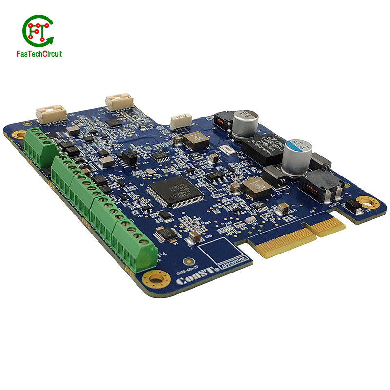
500 series pcb board
Our products are very popular in Togo,United Kingdom,India,Cyprus, the United States and Japan. Won high praise from customers. Based on advanced technology and excellent operations, we provide high-quality overall solutions and world-class services to help customers maintain their competitive advantage in the market. We also provide one-stop OEM service with price advantage and fast delivery!
| Base Material | FR-4/CEM-1/CEM-3/Polyimild/PTFE/Rogers |
| Board Thickness | 0.1-5mm |
| Model Number | Custom PCB & PCB Assembly |
| Type | Aluminum PCB |
| Brand Name | FC |
| Copper Thickness | 0.3-2mil(12-44um) |
| Min. Hole Size | 0.1mm(4mil)for HDI / 0.15mm(6mil) |
| Min. Line Width | 0.075mm/0.075mm(3mil/3mil) |
| Min. Line Spacing | 0.003'' |
| Surface Finishing | HASL/OSP/Ag/ENIG/ENEPIG/Immersion silver/Tin |
| Board Size | Custom |
| Model Number | Customized |
| Base Material | FR4 Aluminum CEM-1 94V0 |
| Surface Finishing | HASLENIG OSP |
| Number of layer | 1-11layer |
| Other service | Components purchasing and assem |
| ly Solder mask | White Black Green Blue,Red,etc. |
| Dsign service | Available |
| Testing | Function testing |
| Certificate | RoHS, ISO/TS16949, ISO9001 |
| Name | High Quality led light aluminum pcb printed circuit board |
| Packaging Details | Vaccum package and standard carton outside High Quality led light aluminum pcb printed circuit board |
| Supply Ability | 44524 Square Meter/Square Meters per Month |
| Quantity (pieces) | > 24991 |
| Lead time (days) | 15 |
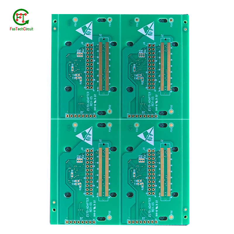
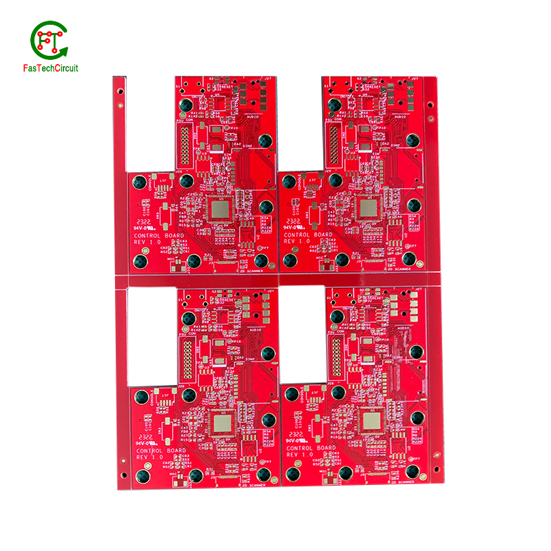
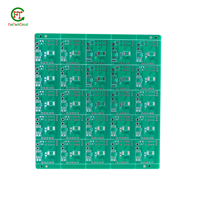
500 series pcb board bearings FAQs Guide Welcome to our state-of-the-art PCB (Printed Circuit Board) products. We are proud to offer a comprehensive range of high-quality and versatile PCB solutions to meet the constantly evolving needs of the modern electronics industry.Our PCBs are expertly designed and manufactured using the latest technology and advanced techniques, ensuring reliability, durability, and exceptional performance for a wide range of applications. We understand the importance of precision and attention to detail in the production of PCBs and we are committed to meeting stringent quality standards.
2.What is the minimum trace width and spacing on a 500 series pcb board?
3.How are holes drilled into a 500 series pcb board?
4.What is the process of etching a 500 series pcb board?
5.What is a 500 series pcb board?
6.How are thermal considerations taken into account during 500 series pcb board design?
7.What is the minimum thickness of a 500 series pcb board?
8.How are 500 series pcb boards protected from environmental factors?
9.How are 500 series pcb boards manufactured?
10.What is the role of a data sheet in 500 series pcb board design?
11.What software is used for 500 series pcb board design?
12.What is the purpose of a 500 series pcb board?
13.How is a 500 series pcb board tested for functionality?
14.What is the maximum size of a 500 series pcb board?
15.Can a 500 series pcb board be used for both power and signal transmission?
1.What is the difference between a diode and a capacitor?
We have a first -class management team, and we pay attention to teamwork to achieve common goals.
A diode is an electronic component that allows current to flow in only one direction. It has two terminals, an anode and a cathode, and works by allowing current to flow from the anode to the cathode, but not in the reverse direction.
A capacitor, on the other hand, is an electronic component that stores electrical energy in an electric field. It has two conductive plates separated by an insulating material, and when a voltage is applied, one plate accumulates a positive charge and the other accumulates a negative charge. This allows the capacitor to store energy and release it when needed.
2.What is the minimum trace width and spacing on a 500 series pcb board?
We operate our 500 series pcb board business with integrity and honesty.
The minimum trace width and spacing on a PCB can vary depending on the manufacturing process and the specific requirements of the design. However, a common industry standard for minimum trace width and spacing is 0.006 inches (0.1524 mm). This is typically used for standard PCBs with a 1 oz copper weight. For more complex designs or higher copper weights, the minimum trace width and spacing may need to be increased to ensure proper functionality and reliability. It is important to consult with the PCB manufacturer and follow their guidelines for minimum trace width and spacing to ensure a successful design.
3.How are holes drilled into a 500 series pcb board?
We actively participate in the 500 series pcb board industry associations and organization activities. The corporate social responsibility performed well, and the focus of brand building and promotion.
Drilling holes into printed circuit boards (PCBs) is a critical part of the PCB manufacturing process. These holes are used for mounting electronic components and for creating electrical connections between different layers of the board. There are two main methods for drilling holes into a PCB – mechanical drilling and laser drilling. Mechanical drilling involves using a high speed drill bit to physically drill through the board, while laser drilling uses a high-powered laser to vaporize the material and create the holes. Both methods have their own advantages and are often used in combination to achieve the desired hole sizes and precision. Regardless of the method, the holes are carefully planned and executed to ensure the successful production of a high-quality PCB.
4.What is the process of etching a 500 series pcb board?
We have flexible production capacity. Whether you are large orders or small orders, you can produce and release goods in a timely manner to meet customer needs.
PCB (Printed Circuit Board) etching is the process of creating a circuit pattern on a copper-clad board by using chemical etchants to selectively remove the unwanted copper. The process begins by transferring the circuit design onto a copper-clad board using various methods such as printing or photolithography. Next, the board is coated with a resist material, which protects the areas of copper that will eventually become the circuit traces. The board is then placed in an etching solution, typically a mixture of acid and water, which dissolves the unprotected copper. Once the desired circuit pattern is etched into the board, the resist material is removed, and the board is cleaned and inspected for any imperfections. PCB etching is a crucial step in the manufacturing of PCBs, as it creates the necessary conductive pathways for electronic components to be mounted and interconnected, making it an essential process in the production of electronic devices.
5.What is a 500 series pcb board?
We pay attention to user experience and product quality, and provide the best product quality and lowest production cost for cooperative customers.
A PCB (Printed Circuit Board) is a flat board made of non-conductive material, such as fiberglass, with conductive pathways etched or printed onto it. It is used to mechanically support and electrically connect electronic components using conductive tracks, pads, and other features etched from copper sheets laminated onto a non-conductive substrate. PCBs are commonly used in electronic devices such as computers, smartphones, and televisions to provide a platform for the components to be mounted and connected together. They are also used in a variety of other applications, including automotive, aerospace, and medical devices.
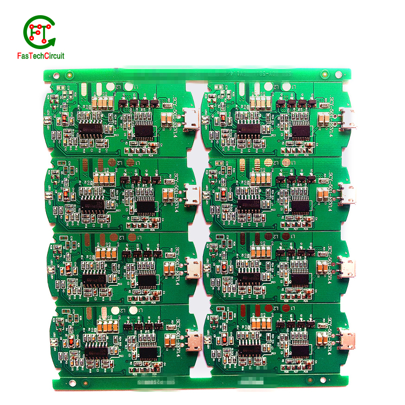
6.How are thermal considerations taken into account during 500 series pcb board design?
As one of the top 500 series pcb board manufacturers in China, we take this very seriously.
Thermal considerations are crucial in the design of printed circuit boards (PCB), as excessive heat can greatly affect the performance and lifespan of electronic components. PCB design engineers must carefully consider thermal management strategies, such as proper placement of heat-generating components, effective heat dissipation techniques, and optimal selection of materials. Thermal simulations and analysis are also commonly used to evaluate and optimize the PCB design to ensure that the temperature of the PCB and its components are within safe limits. By taking into account these thermal considerations, the finished PCB can perform reliably and efficiently, ensuring the overall quality and function of electronic devices.
7.What is the minimum thickness of a 500 series pcb board?
We are committed to providing personalized solutions and established long -term strategic cooperative relationships with customers.
The minimum thickness of a PCB (printed circuit board) can vary depending on the materials and manufacturing processes used. However, the standard minimum thickness for a single-sided PCB is 0.6mm (0.024 inches) and for a double-sided PCB it is 0.8mm (0.032 inches). Thinner PCBs can be made, but they may be more fragile and have limitations on the components and circuitry that can be used.
8.How are 500 series pcb boards protected from environmental factors?
We have established long-term and stable partnerships with our suppliers, so we have great advantages in price and cost and quality assurance.
PCBs, or printed circuit boards, are protected from environmental factors through the use of various techniques and materials. One method is to coat the PCB with a layer of conformal coating, which is a thin layer of protective material that covers the components and circuitry on the board. This coating can protect the PCB from moisture, dust, and other contaminants that could cause damage.
In addition to conformal coating, PCBs can also be protected through designing the layout of the board in a way that minimizes exposure to environmental factors. This includes placing sensitive components in areas that are less susceptible to moisture or temperature changes, as well as using specialized materials that are resistant to the effects of heat, humidity, and other environmental conditions.
9.How are 500 series pcb boards manufactured?
We have the leading technology and innovation capabilities, and attach importance to employee training and development, and provide promotion opportunities.
PCB are manufactured through a series of steps starting with designing the circuit layout. Once the design is finalized, the layout is printed on a special type of paper known as the “artwork”. This artwork is then transferred onto a copper-coated laminate board through a process called etching. The excess copper is removed, leaving behind the desired circuit pattern. The board is then drilled to create holes for components to be inserted. The next step involves adding a thin layer of solder mask to protect the circuit and adding a thin layer of copper to create traces. Finally, the components are added using a specialized machine, and the board goes through a series of tests to ensure proper functionality. Once the tests are passed, the board is cut and separated into individual PCBs for use in various electronic devices.
10.What is the role of a data sheet in 500 series pcb board design?
A data sheet is an essential tool for PCB design, providing vital information and specifications for all of the components used in the design process. It contains detailed technical data, such as dimensions, electrical ratings, and performance characteristics, that allow designers to make informed decisions when selecting and placing components on a PCB. By referencing the data sheet, designers can ensure that each component is properly integrated into the overall design, following any necessary guidelines or restrictions. Additionally, data sheets also provide necessary information for the layout and routing of traces on the PCB, ensuring that the design can meet required performance specifications.

11.What software is used for 500 series pcb board design?
Our 500 series pcb board products have competitive and differentiated advantages, and actively promote digital transformation and innovation.
Some popular software used for PCB design include:
1. Altium Designer
2. Eagle PCB
3. KiCad
4. OrCAD
5. PADS
6. Proteus
7. DipTrace
8. EasyEDA
9. CircuitMaker
10. DesignSpark PCB
12.What is the purpose of a 500 series pcb board?
We pay attention to the transformation of intellectual property protection and innovation achievements. Your OEM or ODM order design we have a complete confidentiality system.
A PCB (Printed Circuit Board) is a flat board made of non-conductive material, such as fiberglass, with conductive pathways etched or printed onto it. The main purpose of a PCB is to provide a platform for electronic components to be mounted and connected together to form a functioning electronic circuit. It serves as a physical support for the components and provides a means for them to communicate with each other through the conductive pathways. PCBs are used in a wide range of electronic devices, from simple household appliances to complex computer systems, and are essential for the proper functioning and reliability of these devices. They also allow for easier and more efficient production of electronic devices, as the components can be mounted and connected in a standardized and automated manner.
13.How is a 500 series pcb board tested for functionality?
A PCB, or Printed Circuit Board, is tested for functionality to ensure that all components and connections on the board are working correctly. This is important in order to detect any potential manufacturing or design defects that could compromise the board's performance. To test a PCB, a range of diagnostic tools and techniques are used including visual inspection, automated testing software, and specialized equipment such as oscilloscopes and multimeters. Experienced technicians also use their knowledge and expertise to troubleshoot and identify any issues with the board. Through this rigorous testing process, any faults or failures are identified and resolved before the PCB is released for production, ensuring that it meets the desired functionality and performance standards.
14.What is the maximum size of a 500 series pcb board?
We pay attention to the introduction and training of talents, scientifically regulate the management system, and focus on cultural construction and team cohesion.
The maximum size of a PCB (printed circuit board) can vary depending on the manufacturer and theircapabilities. However, the industry standard maximum size for a single PCB panel is typically around 18 inches by 24 inches (457 mm by 610 mm). Larger PCBs can be created by combining multiple panels together. Some manufacturers may also have the capability to create custom-sized PCBs that exceed the industry standard maximum size.
15.Can a 500 series pcb board be used for both power and signal transmission?
Yes, a PCB (printed circuit board) can be used for both power and signal transmission. This is commonly seen in electronic devices such as computers, smartphones, and other electronic devices. The PCB acts as a platform for connecting various components and circuits, including power sources and signal pathways. The power and signal traces on the PCB are designed to handle different levels of current and voltage to ensure efficient transmission and prevent interference between the two. However, it is important to properly design and layout the PCB to ensure proper separation and isolation of power and signal traces to avoid any potential issues.
RELATED PRODUCTS & SERVICE
pcb board manufacturing How To Contact US
PCB from 1 to 30 layers, HDI, Heavy Copper, Rigid-flex board with "pcb board manufacturing One-Stop" service.

