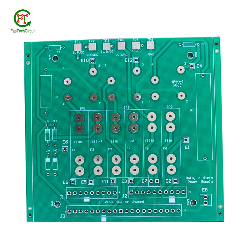
8 layer pcb board
| Number of Layers | 4 layer |
| Base Material | gold sinking |
| Board Thickness | 3.1MM |
| Board Size | 285M*578MM |
| Model Number | 4 layer pcb |
| Type | pcb |
| Place of Origin | Original |
| Brand Name | Original |
| Copper Thickness | 3OZ |
| Min. Hole Size | custom made |
| Min. Line Width | custom made |
| Min. Line Spacing | custom made |
| Surface Finishing | custom made |
| Impedance control | +/- 10% |
| Warpage | less than 1% |
| Packaging Details | New and Original, factory sealed packing, it will be pack in one of these packing type: Tube, Tray, Tape and Reel, Tape and Box, Bulk packing, Bag and etc. Please kindly contact us for more details. |
| Supply Ability | 6373 Piece/Pieces per Week |
| Quantity (pieces) | > 17954 |
| Lead time (days) | 7 |
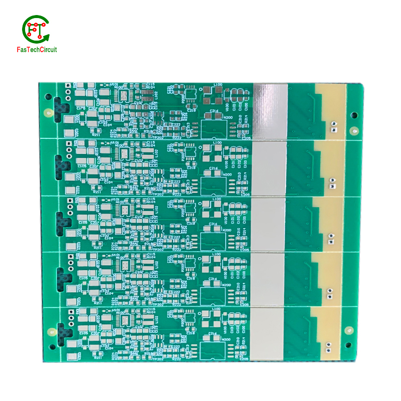
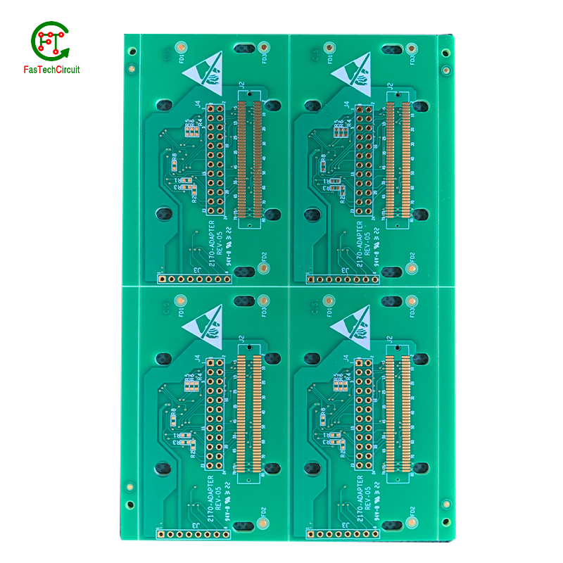
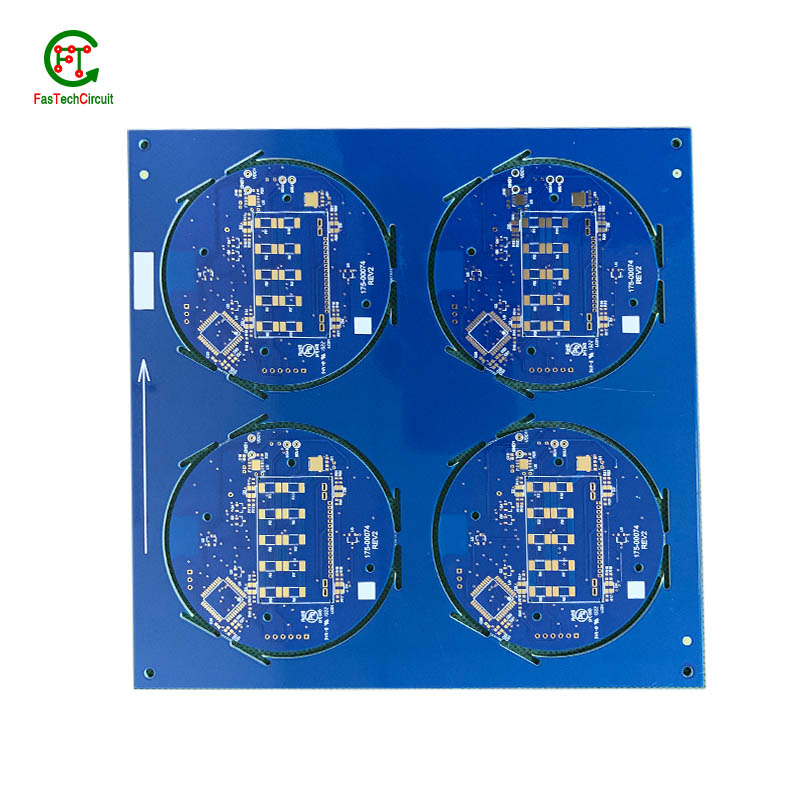
8 layer pcb board bearings FAQs Guide Welcome to our state-of-the-art PCB (Printed Circuit Board) products. We are proud to offer a comprehensive range of high-quality and versatile PCB solutions to meet the constantly evolving needs of the modern electronics industry.Our PCBs are expertly designed and manufactured using the latest technology and advanced techniques, ensuring reliability, durability, and exceptional performance for a wide range of applications. We understand the importance of precision and attention to detail in the production of PCBs and we are committed to meeting stringent quality standards.
2.How are signal integrity issues addressed in 8 layer pcb board design?
3.What is the purpose of a ground plane on a 8 layer pcb board?
4.How does a 8 layer pcb board work?
5.What are the benefits of using surface mount technology (SMT) for 8 layer pcb board?
6.How are power and ground planes connected on a 8 layer pcb board?
7.What is the maximum size of a 8 layer pcb board?
8.What is embedded 8 layer pcb board technology?
9.What is the process of etching a 8 layer pcb board?
10.What is the role of silkscreen on a 8 layer pcb board?
11.How are high-speed/high-frequency 8 layer pcb board tested and validated?
12.What materials are used to make a 8 layer pcb board?
13.What type of solder is used for 8 layer pcb board assembly?
1.What is the power rating for a 8 layer pcb board?
We maintain a certain amount of R&D investment every year and continuously improve operational efficiency to provide better services to our cooperative customers.
The power rating for a PCB (printed circuit board) can vary greatly depending on its size, design, and intended use. Generally, the power rating for a PCB is determined by the maximum amount of current it can safely handle without overheating or causing damage. This can range from a few milliamps for small, low-power circuits to several amps for larger, high-power circuits. It is important to consult the manufacturer's specifications or consult with an engineer to determine the specific power rating for a particular PCB.
2.How are signal integrity issues addressed in 8 layer pcb board design?
We focus on our customers' needs and strive to meet their expectations, so we take this very seriously.
Signal integrity issues are a common concern in PCB design, as they can greatly affect the performance and reliability of electronic systems. These issues arise from high-speed signal transmissions on the board, which can result in degraded signals, data errors, and even system failures. In order to address these issues, PCB designers must consider various factors such as layout, routing, and component placement to ensure proper signal integrity. This involves implementing signal protection measures such as controlled impedance routing, signal shielding, and minimizing signal crosstalk. Additionally, designers may use simulation and analysis tools to identify and resolve any potential signal integrity problems before the PCB goes into production. By carefully addressing signal integrity issues in the design phase, PCBs can achieve optimal performance and functionality.
3.What is the purpose of a ground plane on a 8 layer pcb board?
I have a comprehensive after -sales service system, which can pay attention to market trends in time and adjust our strategy in a timely manner.
A decoupling capacitor is an essential component on a PCB (Printed Circuit Board) which is used to reduce or eliminate high frequency noise between different components. It acts as a buffer between the power supply and other circuit components, by storing electrical charge and then releasing it when there is a sudden change in the supply voltage. This helps to stabilize the power supply, providing a steady and noise-free flow of electricity to the circuit. Furthermore, decoupling capacitors also help to filter out any unwanted signals that may cause interference or disruptions in the proper functioning of the circuit.
4.How does a 8 layer pcb board work?
We maintain a stable growth through reasonable capital operations, focus on industry development trends and cutting -edge technologies, and focus on product quality and safety performance.
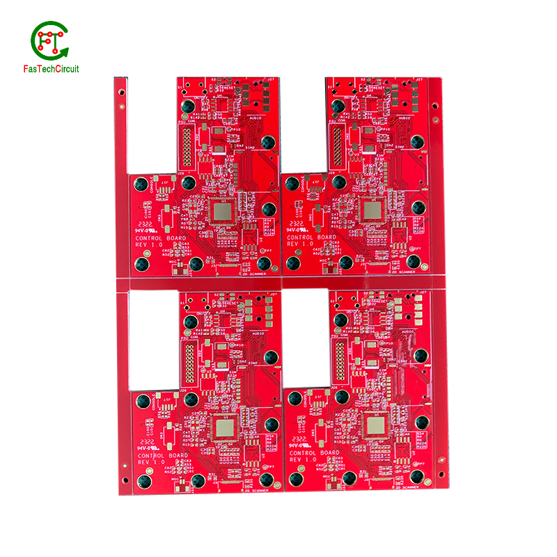
A PCB (Printed Circuit Board) is a thin board made of non-conductive material, such as fiberglass or plastic, with conductive pathways etched or printed onto its surface. These pathways, also known as traces, are used to connect electronic components on the board, such as resistors, capacitors, and integrated circuits.
The PCB works by providing a platform for the components to be mounted and connected in a specific circuit configuration. The traces on the board act as wires, allowing electricity to flow between the components and creating a complete circuit.
The process of creating a PCB involves several steps, including designing the circuit layout, printing or etching the traces onto the board, and attaching the components using soldering techniques. Once the components are attached, the board is tested to ensure that all connections are correct and functioning properly.
When a PCB is connected to a power source, electricity flows through the traces, powering the components and allowing them to perform their intended functions. The traces also act as a pathway for signals to travel between components, allowing for communication and data transfer within the circuit.
PCBs are used in a wide range of electronic devices, from simple household appliances to complex computer systems. They provide a compact and efficient way to connect and control electronic components, making them an essential part of modern technology.
5.What are the benefits of using surface mount technology (SMT) for 8 layer pcb board?
We focus on innovation and continuous improvement to maintain a competitive advantage.
Surface mount technology (SMT) is a popular method for assembling printed circuit boards (PCBs) that offers numerous benefits over traditional through-hole components. Firstly, SMT components are smaller and more compact, allowing for greater PCB density and reducing the overall size of the board. This makes SMT ideal for increasingly miniaturized electronics, such as smartphones and wearables. Additionally, SMT components are typically cheaper and easier to manufacture, leading to cost savings in both materials and labor. SMT also allows for automated assembly, resulting in faster and more efficient production processes. Furthermore, the smaller size of SMT components leads to improved electrical performance due to decreased parasitic effects and shorter signal paths. This makes SMT ideal for high-frequency applications.
6.How are power and ground planes connected on a 8 layer pcb board?
Power and ground planes are typically connected on a PCB through vias, which are small holes drilled through the layers of the PCB. These vias are filled with conductive material, such as copper, and allow for the flow of current between the power and ground planes. The vias are strategically placed throughout the PCB to ensure a low impedance connection between the power and ground planes. Additionally, traces or copper pours can also be used to connect the power and ground planes on different layers of the PCB.
7.What is the maximum size of a 8 layer pcb board?
We pay attention to the introduction and training of talents, scientifically regulate the management system, and focus on cultural construction and team cohesion.
The maximum size of a PCB (printed circuit board) can vary depending on the manufacturer and theircapabilities. However, the industry standard maximum size for a single PCB panel is typically around 18 inches by 24 inches (457 mm by 610 mm). Larger PCBs can be created by combining multiple panels together. Some manufacturers may also have the capability to create custom-sized PCBs that exceed the industry standard maximum size.
8.What is embedded 8 layer pcb board technology?
Our products & services cover a wide range of areas and meet the needs of different fields.
Embedded PCB technology refers to the integration of electronic components directly onto a printed circuit board (PCB) during the manufacturing process. This allows for a more compact and efficient design, as well as improved reliability and performance. The components are embedded within the layers of the PCB, rather than being mounted on the surface, resulting in a more streamlined and durable product. This technology is commonly used in applications such as smartphones, tablets, and other portable electronic devices.
9.What is the process of etching a 8 layer pcb board?
We have flexible production capacity. Whether you are large orders or small orders, you can produce and release goods in a timely manner to meet customer needs.
PCB (Printed Circuit Board) etching is the process of creating a circuit pattern on a copper-clad board by using chemical etchants to selectively remove the unwanted copper. The process begins by transferring the circuit design onto a copper-clad board using various methods such as printing or photolithography. Next, the board is coated with a resist material, which protects the areas of copper that will eventually become the circuit traces. The board is then placed in an etching solution, typically a mixture of acid and water, which dissolves the unprotected copper. Once the desired circuit pattern is etched into the board, the resist material is removed, and the board is cleaned and inspected for any imperfections. PCB etching is a crucial step in the manufacturing of PCBs, as it creates the necessary conductive pathways for electronic components to be mounted and interconnected, making it an essential process in the production of electronic devices.
10.What is the role of silkscreen on a 8 layer pcb board?
Being one of the top 8 layer pcb board manufacturers in China, We attach great importance to this detail.
Silkscreen, also known as legend or nomenclature, is a vital component of a printed circuit board (PCB). It is the layer of text and symbols that are printed on the surface of the PCB to provide essential information for component placement and identification. The silkscreen plays a crucial role in the manufacturing process of PCBs, as it helps to ensure the accuracy and functionality of the final product. By indicating component locations, values, and reference designators, the silkscreen serves as a guide for the assembly and soldering of electronic components. Additionally, it also provides important information for maintenance and troubleshooting purposes.
11.How are high-speed/high-frequency 8 layer pcb board tested and validated?
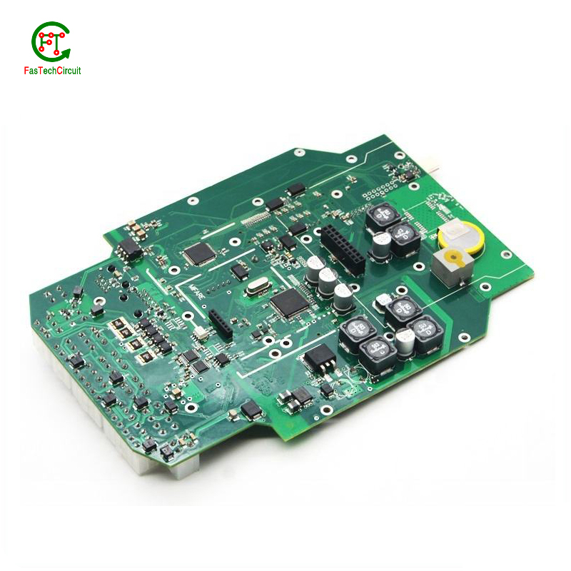
Testing and validation are essential steps in the production process of high-speed and high-frequency printed circuit boards (PCBs). These specialized types of PCBs are used in a wide range of industries, including telecommunications, aerospace, and automotive, and require precision and reliability in their performance.
The testing and validation process for high-speed/high-frequency PCBs involves several steps to ensure that the final product meets the required specifications. This starts with design simulation and analysis using specialized software to verify the layout and electrical characteristics of the PCB.
Once the design is confirmed, prototype PCBs are manufactured and subjected to various tests, including signal integrity and power integrity tests. These tests evaluate the electrical performance of the PCB, such as its ability to transmit signals at high speeds and maintain signal integrity.
In addition to electrical tests, environmental and mechanical tests are also performed to assess the durability and reliability of the PCB under different conditions, such as temperature changes and mechanical stress.
The final step in the testing and validation process is the inspection and analysis of the tested PCBs. This involves a detailed review of the test results and any necessary modifications to meet the required specifications.
12.What materials are used to make a 8 layer pcb board?
We have advanced production equipment and technology to meet the needs of customers, and can provide customers with high quality, low priced 8 layer pcb board products.
A PCB, or printed circuit board, is typically made of a non-conductive material such as fiberglass or composite epoxy resin. This material acts as a base for a thin layer of copper foil, which is then etched to create the desired circuit pattern. Other common materials used in the production of PCBs include solder mask, a polymer layer used to insulate and protect the copper traces, and silkscreen, which is used to label and identify the different components on the PCB. In addition, various electronic components such as resistors, capacitors, and diodes are also mounted onto the PCB to form a functional electronic circuit. Other potential materials used in the production of PCBs include metal core, ceramics, and conductive ink, depending on the specific design and requirements of the circuit.
13.What type of solder is used for 8 layer pcb board assembly?
The most commonly used solder for PCB assembly is a lead-free solder, specifically a tin-silver-copper (SnAgCu) alloy. This type of solder is preferred due to its high melting point, good wetting properties, and compatibility with surface mount technology (SMT) components. Other types of solder that may be used include tin-lead (SnPb) solder and lead-free alternatives such as tin-copper (SnCu) and tin-bismuth (SnBi) alloys. The specific type of solder used may vary depending on the application and industry standards.
RELATED PRODUCTS & SERVICE
pcb board manufacturing How To Contact US
PCB from 1 to 30 layers, HDI, Heavy Copper, Rigid-flex board with "pcb board manufacturing One-Stop" service.

