about pcb design and make
Our managers and technicians are all experienced personnel who have been engaged in the PCB industry for more than 20 years, so we have rich production management experience and professional PCB skills. We constantly introduce new equipment, new technologies, and use high-quality materials to ensure the quality of PCB products. We have professional technical personnel who can provide early design consultation and technical support, making customers more worry-free. With high-quality and reliable products, advanced technology and value-added services, our products are very popular in Brazil,United States of America,Central African Republic,Croatia,Chad,Bahrain, the United States and Japan. Won high praise from customers.
| Base Material | FR-4/CEM-1/CEM-3/Polyimild/PTFE/Rogers |
| Board Thickness | 0.2-8mm |
| Model Number | Custom PCB & PCB Assembly |
| Type | Aluminum PCB |
| Brand Name | FC |
| Copper Thickness | 0.5-2mil(8-44um) |
| Min. Hole Size | 0.1mm(4mil)for HDI / 0.15mm(6mil) |
| Min. Line Width | 0.075mm/0.075mm(3mil/3mil) |
| Min. Line Spacing | 0.003'' |
| Surface Finishing | HASL/OSP/Ag/ENIG/ENEPIG/Immersion silver/Tin |
| Board Size | Custom |
| Model Number | Customized |
| Base Material | FR4 Aluminum CEM-1 94V0 |
| Surface Finishing | HASLENIG OSP |
| Number of layer | 1-12layer |
| Other service | Components purchasing and assem |
| ly Solder mask | White Black Green Blue,Red,etc. |
| Dsign service | Available |
| Testing | Function testing |
| Certificate | RoHS, ISO/TS16949, ISO9001 |
| Name | High Quality led light aluminum pcb printed circuit board |
| Packaging Details | Vaccum package and standard carton outside High Quality led light aluminum pcb printed circuit board |
| Supply Ability | 49690 Square Meter/Square Meters per Month |
| Quantity (pieces) | > 14740 |
| Lead time (days) | 7 |
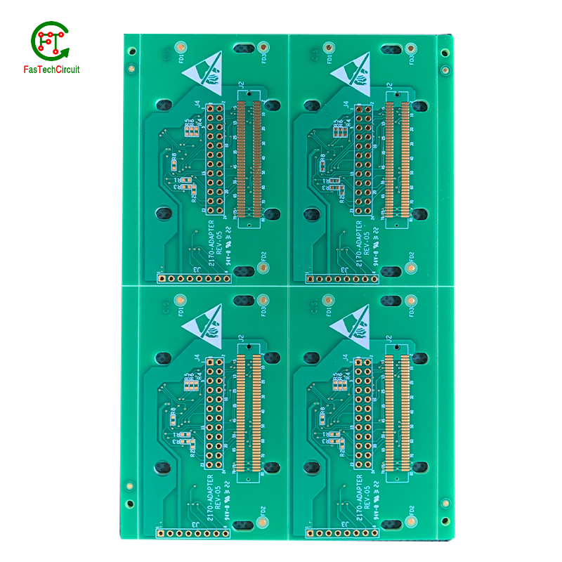
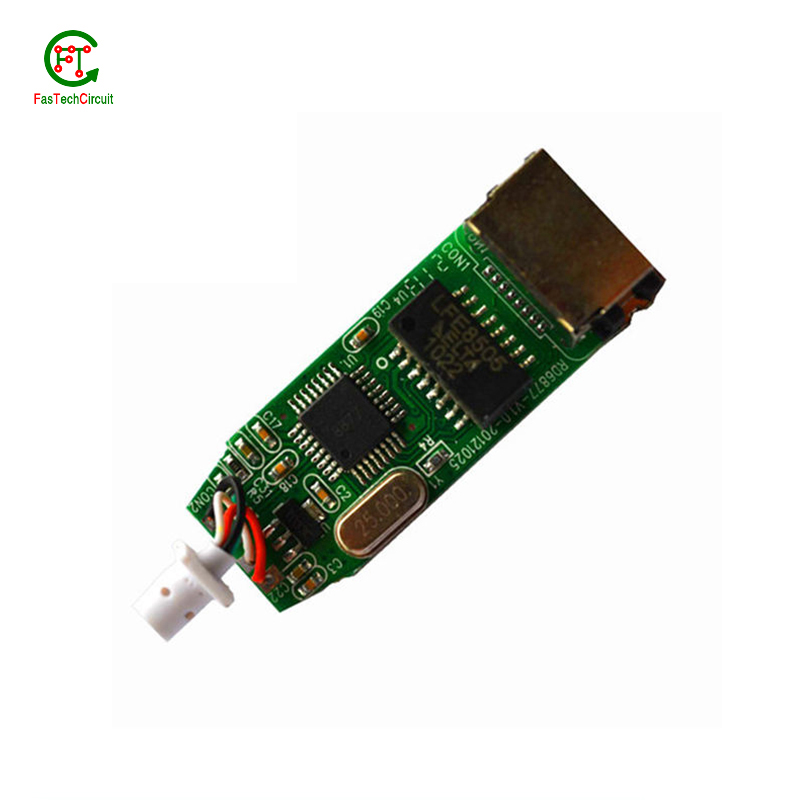
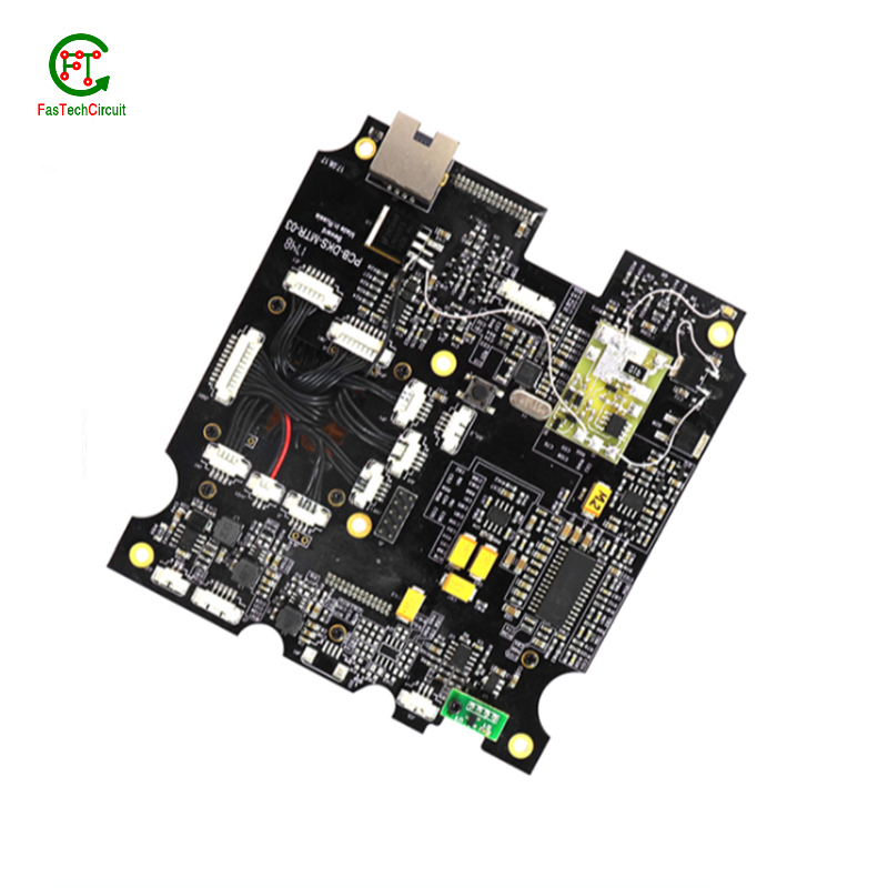
about pcb design and make bearings FAQs Guide Welcome to our state-of-the-art PCB (Printed Circuit Board) products. We are proud to offer a comprehensive range of high-quality and versatile PCB solutions to meet the constantly evolving needs of the modern electronics industry.Our PCBs are expertly designed and manufactured using the latest technology and advanced techniques, ensuring reliability, durability, and exceptional performance for a wide range of applications. We understand the importance of precision and attention to detail in the production of PCBs and we are committed to meeting stringent quality standards.
2.What is the difference between a gold-plated and a tin-plated about pcb design and make?
3.What is the purpose of a ground plane on a about pcb design and make?
4.Can a about pcb design and make be used for both power and signal transmission?
5.What are the advantages of using a about pcb design and make?
6.Can about pcb design and makes be used for high-speed data transmission?
7.How are about pcb design and makes protected from environmental factors?
8.Can about pcb design and makes be used in high voltage applications?
9.What is the role of silkscreen on a about pcb design and make?
10.What type of material is used for the silkscreen on a about pcb design and make?
11.What are some common about pcb design and make layout guidelines?
12.What is the future outlook for about pcb design and make technology?
13.What is the function of a resistor on a about pcb design and make?
1.How are about pcb design and makes tested for quality control?
We have broad development space in domestic and foreign markets. about pcb design and make have great advantages in terms of price, quality, and delivery date.
PCB (Printed Circuit Board) testing is a critical step in the quality control process of electronic products. It ensures that all components and connections on the board are functioning correctly and that the PCB meets the required standards and specifications.
The testing process typically starts with a visual inspection to identify any visible defects, such as incorrect soldering or damaged components. Next, electrical testing is conducted to check the functionality of each individual component and the overall circuit.
One common method of testing is the use of a test fixture, which applies signals to the PCB and checks for correct responses. Other methods include automated optical inspection (AOI) and in-circuit testing (ICT).
Once the initial testing is completed, the PCB may undergo environmental testing to simulate real-life conditions and ensure its reliability and durability. This includes temperature and humidity cycling, vibration and shock testing, and more.
2.What is the difference between a gold-plated and a tin-plated about pcb design and make?
A gold-plated PCB (Printed Circuit Board) is a type of PCB that has a thin layer of gold coating on its surface. This layer is added through a process called electroplating and is commonly used to protect the PCB components from corrosion and increase the conductivity. On the other hand, a tin-plated PCB has a layer of tin coating on its surface, which is also applied through electroplating. Unlike gold plating, tin plating is mainly used to prevent oxidization and improve solderability.
3.What is the purpose of a ground plane on a about pcb design and make?
I have a comprehensive after -sales service system, which can pay attention to market trends in time and adjust our strategy in a timely manner.
A decoupling capacitor is an essential component on a PCB (Printed Circuit Board) which is used to reduce or eliminate high frequency noise between different components. It acts as a buffer between the power supply and other circuit components, by storing electrical charge and then releasing it when there is a sudden change in the supply voltage. This helps to stabilize the power supply, providing a steady and noise-free flow of electricity to the circuit. Furthermore, decoupling capacitors also help to filter out any unwanted signals that may cause interference or disruptions in the proper functioning of the circuit.
4.Can a about pcb design and make be used for both power and signal transmission?
Yes, a PCB (printed circuit board) can be used for both power and signal transmission. This is commonly seen in electronic devices such as computers, smartphones, and other electronic devices. The PCB acts as a platform for connecting various components and circuits, including power sources and signal pathways. The power and signal traces on the PCB are designed to handle different levels of current and voltage to ensure efficient transmission and prevent interference between the two. However, it is important to properly design and layout the PCB to ensure proper separation and isolation of power and signal traces to avoid any potential issues.
5.What are the advantages of using a about pcb design and make?
We are centered on customers and always pay attention to customers' needs for about pcb design and make products.
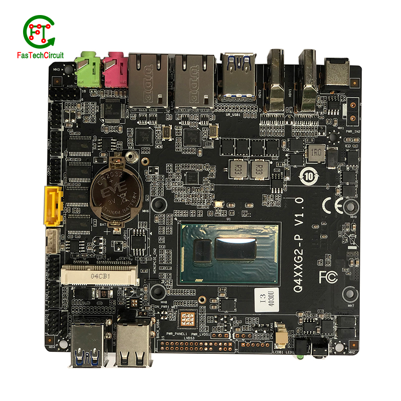
There are several advantages of using a PCB (Printed Circuit Board). Firstly, a PCB provides a compact and organized layout for electronic components, which makes it easier for technicians to troubleshoot and repair any issues. Secondly, it reduces the chances of loose connections and short circuits, which can be a major safety concern. Thirdly, PCBs are cost-effective and can be easily mass-produced, making them a popular choice for large-scale production. Additionally, they offer durability and stability, ensuring long-lasting performance. Finally, PCBs also allow for easy integration of new components, making it easier to upgrade or modify the electronic devices.
6.Can about pcb design and makes be used for high-speed data transmission?
Yes, PCBs (printed circuit boards) can be used for high-speed data transmission. PCBs are commonly used in electronic devices and systems to connect and route electrical signals between components. They are designed to have specific trace widths, lengths, and impedance to ensure efficient and reliable transmission of high-speed signals. Additionally, PCBs can be designed with specialized materials and techniques, such as controlled impedance and differential signaling, to further optimize their performance for high-speed data transmission.
7.How are about pcb design and makes protected from environmental factors?
We have established long-term and stable partnerships with our suppliers, so we have great advantages in price and cost and quality assurance.
PCBs, or printed circuit boards, are protected from environmental factors through the use of various techniques and materials. One method is to coat the PCB with a layer of conformal coating, which is a thin layer of protective material that covers the components and circuitry on the board. This coating can protect the PCB from moisture, dust, and other contaminants that could cause damage.
In addition to conformal coating, PCBs can also be protected through designing the layout of the board in a way that minimizes exposure to environmental factors. This includes placing sensitive components in areas that are less susceptible to moisture or temperature changes, as well as using specialized materials that are resistant to the effects of heat, humidity, and other environmental conditions.
8.Can about pcb design and makes be used in high voltage applications?
We have advantages in marketing and channel expansion. Suppliers have established good cooperative relations, continuously improved workflows, improved efficiency and productivity, and provided customers with high -quality products and services.
Yes, PCBs (printed circuit boards) can be used in high voltage applications. However, the design and construction of the PCB must be carefully considered to ensure it can withstand the high voltage without causing damage or malfunction. This may include using specialized materials, increasing the spacing between components, and implementing proper insulation and grounding techniques. It is important to consult with a qualified engineer or designer when using PCBs in high voltage applications to ensure safety and reliability.
9.What is the role of silkscreen on a about pcb design and make?
Being one of the top about pcb design and make manufacturers in China, We attach great importance to this detail.
Silkscreen, also known as legend or nomenclature, is a vital component of a printed circuit board (PCB). It is the layer of text and symbols that are printed on the surface of the PCB to provide essential information for component placement and identification. The silkscreen plays a crucial role in the manufacturing process of PCBs, as it helps to ensure the accuracy and functionality of the final product. By indicating component locations, values, and reference designators, the silkscreen serves as a guide for the assembly and soldering of electronic components. Additionally, it also provides important information for maintenance and troubleshooting purposes.
10.What type of material is used for the silkscreen on a about pcb design and make?
We have a wide range of about pcb design and make customer groups and establishes long -term cooperative relationships with partners. The countries we provide services include .
The material used for the silkscreen on a PCB is typically a white or black ink made of epoxy or acrylic. It is applied using a screen printing process and is cured at high temperatures to ensure durability and resistance to chemicals and solvents.
11.What are some common about pcb design and make layout guidelines?
We should have a stable supply chain and logistics capabilities, and provide customers with high -quality, low -priced about pcb design and make products.
Thermal considerations play a crucial role in the design of printed circuit boards (PCBs). The concept of heat management is critical as excessive heat can lead to reduced performance and potential damage to the electronic components on the board. This is why thermal considerations are carefully taken into account during PCB design. Designers must carefully consider factors such as the size, placement, and orientation of components on the board to ensure efficient heat dissipation. They also need to factor in the type and thickness of the board material, as well as incorporate proper ventilation and heat sinks to prevent overheating. By carefully considering these thermal aspects during the design process, the resulting PCBs can perform optimally and have a longer lifespan.
12.What is the future outlook for about pcb design and make technology?
Printed Circuit Boards, or PCBs, have been a vital component in electronic devices for decades. They serve as the foundation for the electrical connections and components that make our devices function properly. As technology continues to advance, so does the demand for smaller, faster, and more efficient PCBs. With the rise of IoT and smart devices, the future outlook for PCB technology is promising. It is expected that PCBs will become even more compact and complex, utilizing advanced materials and techniques such as 3D printing and flexible substrates. This will not only improve the performance of electronic devices, but also make them more durable and cost-effective. Furthermore, as sustainability becomes a growing concern, eco-friendly PCB materials and manufacturing processes are being developed to reduce environmental impact. With these advancements, it is safe to say that the future of PCB technology is bright and full of endless possibilities.
13.What is the function of a resistor on a about pcb design and make?
We are a new about pcb design and make manufacturer.
The ground plane on a printed circuit board (PCB) serves as a reference point for the electrical signals that flow throughout the circuit. It is typically a large area of copper that is connected to the negative terminal of the power supply and serves as a low-impedance return path for current. Its main purpose is to provide a stable and uniform ground connection for the components on the PCB, helping to reduce electromagnetic interference and ensuring proper signal grounding. Without a ground plane, the circuit may experience noise and other unwanted effects, potentially causing malfunctions or disruptions in its functionality. Therefore, the ground plane plays a crucial role in ensuring the overall performance and reliability of a PCB.
RELATED PRODUCTS & SERVICE
pcb board manufacturing How To Contact US
PCB from 1 to 30 layers, HDI, Heavy Copper, Rigid-flex board with "pcb board manufacturing One-Stop" service.

