5050 led pcb assembly
FasTechCircuit has established market development, product development, production engineering, process control, quality assurance, material control, and after-sales service management systems. Our products are widely used in various fields such as communications, industrial control, computer applications, aerospace, military, medical, and testing instruments. We can provide one-stop OEM service with price advantage and fast delivery! Our products h
| Base Material | FR-4/CEM-1/CEM-3/Polyimild/PTFE/Rogers |
| Board Thickness | 0.2-5mm |
| Model Number | Custom PCB & PCB Assembly |
| Type | Aluminum PCB |
| Brand Name | FC |
| Copper Thickness | 0.3-2mil(9-47um) |
| Min. Hole Size | 0.1mm(4mil)for HDI / 0.15mm(6mil) |
| Min. Line Width | 0.075mm/0.075mm(3mil/3mil) |
| Min. Line Spacing | 0.003'' |
| Surface Finishing | HASL/OSP/Ag/ENIG/ENEPIG/Immersion silver/Tin |
| Board Size | Custom |
| Model Number | Customized |
| Base Material | FR4 Aluminum CEM-1 94V0 |
| Surface Finishing | HASLENIG OSP |
| Number of layer | 1-14layer |
| Other service | Components purchasing and assem |
| ly Solder mask | White Black Green Blue,Red,etc. |
| Dsign service | Available |
| Testing | Function testing |
| Certificate | RoHS, ISO/TS16949, ISO9001 |
| Name | High Quality led light aluminum pcb printed circuit board |
| Packaging Details | Vaccum package and standard carton outside High Quality led light aluminum pcb printed circuit board |
| Supply Ability | 54330 Square Meter/Square Meters per Month |
| Quantity (pieces) | > 24577 |
| Lead time (days) | 14 |
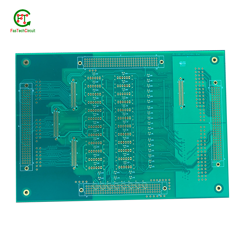
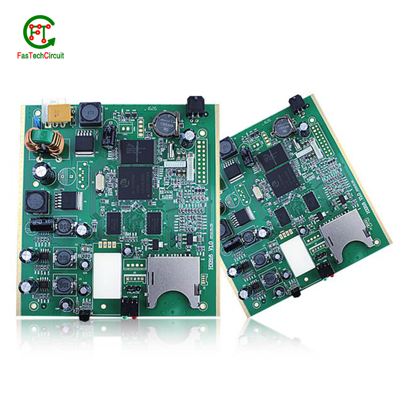
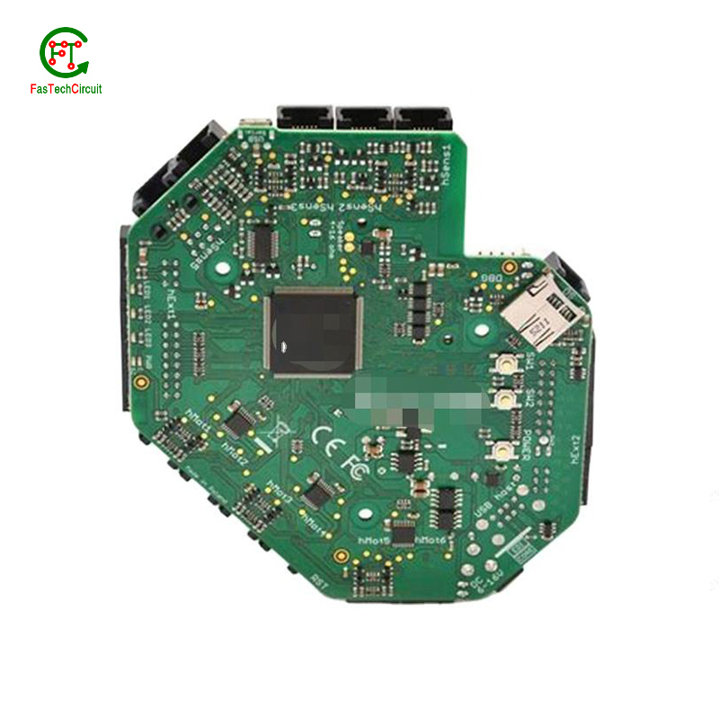
5050 led pcb assembly bearings FAQs Guide Welcome to our state-of-the-art PCB (Printed Circuit Board) products. We are proud to offer a comprehensive range of high-quality and versatile PCB solutions to meet the constantly evolving needs of the modern electronics industry.Our PCBs are expertly designed and manufactured using the latest technology and advanced techniques, ensuring reliability, durability, and exceptional performance for a wide range of applications. We understand the importance of precision and attention to detail in the production of PCBs and we are committed to meeting stringent quality standards.
2.How are high-speed/high-frequency 5050 led pcb assembly tested and validated?
3.How are thermal considerations taken into account during 5050 led pcb assembly design?
4.What is the role of silkscreen on a 5050 led pcb assembly?
5.What is the difference between a copper pour and a trace on a 5050 led pcb assembly?
6.What are the main components of a 5050 led pcb assembly?
7.How are components attached to a 5050 led pcb assembly?
8.What is the purpose of a 5050 led pcb assembly?
9.What is embedded 5050 led pcb assembly technology?
10.What is a through-hole component?
11.What are the advantages of using a 5050 led pcb assembly?
12.What software is used for 5050 led pcb assembly design?
13.What is the maximum operating temperature of a 5050 led pcb assembly?
14.How are 5050 led pcb assembly used in medical devices?
15.Can a 5050 led pcb assembly be used with both through-hole and surface mount components?
1.Can a 5050 led pcb assembly be repaired if damaged?
We focus on teamwork and communication to achieve common goals, We attach great importance to this detail.
Yes, a PCB (printed circuit board) can be repaired if it is damaged. The extent of the damage and the complexity of the circuit will determine the difficulty and feasibility of the repair. Some common methods for repairing a damaged PCB include:
1. Soldering: If the damage is limited to a few components or traces, they can be replaced or repaired by soldering new components or wires onto the board.
2. Trace repair: If a trace (conductive pathway) on the PCB is damaged or broken, it can be repaired by using a conductive ink or wire to bridge the gap.
3. Component replacement: If a specific component on the PCB is damaged, it can be replaced with a new one. This requires identifying the damaged component and sourcing a replacement.
4. PCB rework: In some cases, the entire PCB may need to be reworked, which involves removing and replacing multiple components and traces.
2.How are high-speed/high-frequency 5050 led pcb assembly tested and validated?
Testing and validation are essential steps in the production process of high-speed and high-frequency printed circuit boards (PCBs). These specialized types of PCBs are used in a wide range of industries, including telecommunications, aerospace, and automotive, and require precision and reliability in their performance.
The testing and validation process for high-speed/high-frequency PCBs involves several steps to ensure that the final product meets the required specifications. This starts with design simulation and analysis using specialized software to verify the layout and electrical characteristics of the PCB.
Once the design is confirmed, prototype PCBs are manufactured and subjected to various tests, including signal integrity and power integrity tests. These tests evaluate the electrical performance of the PCB, such as its ability to transmit signals at high speeds and maintain signal integrity.
In addition to electrical tests, environmental and mechanical tests are also performed to assess the durability and reliability of the PCB under different conditions, such as temperature changes and mechanical stress.
The final step in the testing and validation process is the inspection and analysis of the tested PCBs. This involves a detailed review of the test results and any necessary modifications to meet the required specifications.
3.How are thermal considerations taken into account during 5050 led pcb assembly design?
As one of the top 5050 led pcb assembly manufacturers in China, we take this very seriously.
Thermal considerations are crucial in the design of printed circuit boards (PCB), as excessive heat can greatly affect the performance and lifespan of electronic components. PCB design engineers must carefully consider thermal management strategies, such as proper placement of heat-generating components, effective heat dissipation techniques, and optimal selection of materials. Thermal simulations and analysis are also commonly used to evaluate and optimize the PCB design to ensure that the temperature of the PCB and its components are within safe limits. By taking into account these thermal considerations, the finished PCB can perform reliably and efficiently, ensuring the overall quality and function of electronic devices.
4.What is the role of silkscreen on a 5050 led pcb assembly?
Being one of the top 5050 led pcb assembly manufacturers in China, We attach great importance to this detail.
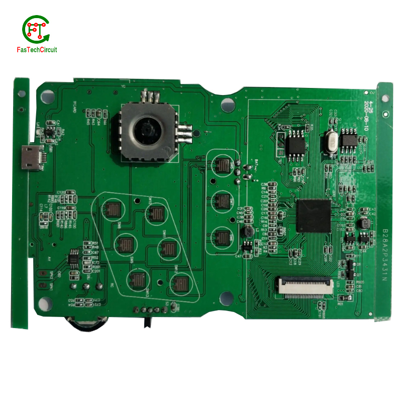
Silkscreen, also known as legend or nomenclature, is a vital component of a printed circuit board (PCB). It is the layer of text and symbols that are printed on the surface of the PCB to provide essential information for component placement and identification. The silkscreen plays a crucial role in the manufacturing process of PCBs, as it helps to ensure the accuracy and functionality of the final product. By indicating component locations, values, and reference designators, the silkscreen serves as a guide for the assembly and soldering of electronic components. Additionally, it also provides important information for maintenance and troubleshooting purposes.
5.What is the difference between a copper pour and a trace on a 5050 led pcb assembly?
We adhere to the principle of quality first and have a complete production quality management system and quality inspection process.
A copper pour and a trace are two common electronic components that are found on a printed circuit board (PCB). A copper pour is a large area of copper that is used to connect multiple components or ground signals together on a PCB. This creates a solid and low resistance pathway for signals to flow. On the other hand, a trace is a thin line of copper used to connect individual components on a PCB. It carries a specific signal from one component to another. Unlike a copper pour, a trace can be designed to carry a specific current and have a specific width to meet the requirements of the circuit.
6.What are the main components of a 5050 led pcb assembly?
We continuously upgrade our skills and knowledge to adapt to changing 5050 led pcb assembly market needs.
A typical PCB consists of several vital components, including a substrate material, copper traces, solder mask, silk screen, and plated through-holes. The substrate material acts as the base and provides mechanical support for the board. Copper traces, usually made of thin lines of copper foil, serve as the conductive paths for transmitting electrical signals. The solder mask, applied as a protective layer, prevents accidental short circuits and corrosion. Silk screen, a layer of ink-based labeling, aids in component identification. Lastly, plated through-holes enable electrical connection between different layers of the PCB board. These components work together to form a fully functioning PCB.
7.How are components attached to a 5050 led pcb assembly?
We adhere to the principle of integrity and transparency, and establish long -term relationships with partners, and we attach great importance to this detail.
eads or pins of the component and melting solder onto them, whicComponents are attached to a PCB (printed circuit board) through a process called soldering. This involves heating the metal lh then solidifies and creates a strong electrical and mechanical connection between the component and the PCB. There are two main methods of soldering components onto a PCB:
1. Through-hole soldering: This method involves inserting the leads or pins of the component through pre-drilled holes on the PCB and soldering them on the opposite side of the board. This method is commonly used for larger components such as resistors, capacitors, and integrated circuits.
2. Surface mount soldering: This method involves soldering the component directly onto the surface of the PCB, without the need for pre-drilled holes. This is done using specialized equipment such as a soldering iron or a reflow oven. Surface mount components are smaller in size and are commonly used for more complex and compact electronic devices.
8.What is the purpose of a 5050 led pcb assembly?
We pay attention to the transformation of intellectual property protection and innovation achievements. Your OEM or ODM order design we have a complete confidentiality system.
A PCB (Printed Circuit Board) is a flat board made of non-conductive material, such as fiberglass, with conductive pathways etched or printed onto it. The main purpose of a PCB is to provide a platform for electronic components to be mounted and connected together to form a functioning electronic circuit. It serves as a physical support for the components and provides a means for them to communicate with each other through the conductive pathways. PCBs are used in a wide range of electronic devices, from simple household appliances to complex computer systems, and are essential for the proper functioning and reliability of these devices. They also allow for easier and more efficient production of electronic devices, as the components can be mounted and connected in a standardized and automated manner.
9.What is embedded 5050 led pcb assembly technology?
Our products & services cover a wide range of areas and meet the needs of different fields.
Embedded PCB technology refers to the integration of electronic components directly onto a printed circuit board (PCB) during the manufacturing process. This allows for a more compact and efficient design, as well as improved reliability and performance. The components are embedded within the layers of the PCB, rather than being mounted on the surface, resulting in a more streamlined and durable product. This technology is commonly used in applications such as smartphones, tablets, and other portable electronic devices.
10.What is a through-hole component?
We focus on providing high 5050 led pcb assembly quality products and services.
A through-hole component is an electronic component that has leads or pins that are inserted into holes on a printed circuit board (PCB) and then soldered to the opposite side of the board. This type of component is typically larger and more robust than surface mount components, and is often used for high-power or high-voltage applications. Through-hole components are also easier to replace or repair compared to surface mount components.
11.What are the advantages of using a 5050 led pcb assembly?
We are centered on customers and always pay attention to customers' needs for 5050 led pcb assembly products.
There are several advantages of using a PCB (Printed Circuit Board). Firstly, a PCB provides a compact and organized layout for electronic components, which makes it easier for technicians to troubleshoot and repair any issues. Secondly, it reduces the chances of loose connections and short circuits, which can be a major safety concern. Thirdly, PCBs are cost-effective and can be easily mass-produced, making them a popular choice for large-scale production. Additionally, they offer durability and stability, ensuring long-lasting performance. Finally, PCBs also allow for easy integration of new components, making it easier to upgrade or modify the electronic devices.
12.What software is used for 5050 led pcb assembly design?
Our 5050 led pcb assembly products have competitive and differentiated advantages, and actively promote digital transformation and innovation.
Some popular software used for PCB design include:
1. Altium Designer
2. Eagle PCB
3. KiCad
4. OrCAD
5. PADS
6. Proteus
7. DipTrace
8. EasyEDA
9. CircuitMaker
10. DesignSpark PCB
13.What is the maximum operating temperature of a 5050 led pcb assembly?
We have a professional team that is committed to the innovation and development of 5050 led pcb assembly.
The maximum operating temperature of a PCB (printed circuit board) can vary depending on the materials and components used in its construction. Generally, the maximum operating temperature for a standard FR4 PCB is around 130-140 degrees Celsius. However, specialized materials such as high-temperature laminates or ceramic substrates can withstand higher temperatures up to 200-250 degrees Celsius. The maximum operating temperature of a PCB should always be determined by the manufacturer's specifications and guidelines.
14.How are 5050 led pcb assembly used in medical devices?
Printed Circuit Boards (PCBs) are essential components used in a wide range of medical devices, playing a crucial role in both diagnostic and treatment equipment. These devices require reliable and precise circuitry to accurately collect and process data, deliver therapies, and regulate medical procedures. PCBs are used in equipment such as MRI machines, pacemakers, defibrillators, and monitors, where their small size and high density make them ideal for compact and portable designs. In addition, PCBs are also used in medical implants, enabling a safe and secure connection between the device and the body. With their advanced technology, PCBs continue to be an integral part of the medical industry, ensuring the effectiveness and success of various medical procedures and treatments.
15.Can a 5050 led pcb assembly be used with both through-hole and surface mount components?
We continue to improve 5050 led pcb assembly products and processes to improve efficiency.
Yes, a PCB (printed circuit board) can be designed to accommodate both through-hole and surface mount components. This is known as a mixed-technology PCB. The PCB will have both through-hole and surface mount pads and traces, allowing for the placement and soldering of both types of components. This type of PCB is commonly used in electronic devices that require a combination of through-hole and surface mount components for functionality.
RELATED PRODUCTS & SERVICE
pcb board manufacturing How To Contact US
PCB from 1 to 30 layers, HDI, Heavy Copper, Rigid-flex board with "pcb board manufacturing One-Stop" service.

