94v0 pcb 1-layer pcb board
| Model Number | customized PCBA |
| Type | pcba |
| Place of Origin | Guangdong, China |
| Brand Name | none |
| Copper Thickness | 1 oz |
| Supplier Type | OEM |
| Application | Electronics Device |
| Service | One-step Service |
| Layer | 1-50layers |
| Solder mask color | Blue.green.red.black.white.etc |
| Testing Service | 100% |
| Component size | 0201-1127mm |
| Component max height | 26mm |
| Min lead pitch | 0.4mm |
| Min BGA ball pitch | 0.3mm |
| Max PCB size | 443x475mm |
| Packaging Details | Vacuum package for bare PCB and ESD package for PCBA Printed Circuit Board Factory FPC Board PCBA Companies PCBA Assembly |
| Supply Ability | 47910 Piece/Pieces per Week |
| Quantity (pieces) | > 732 |
| Lead time (days) | 12 |
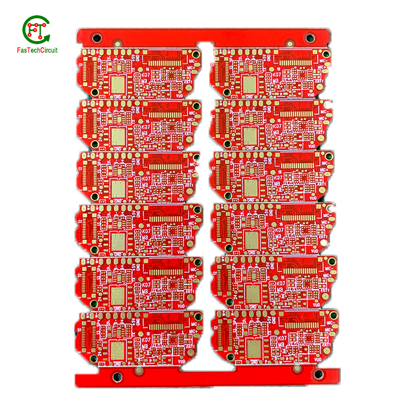
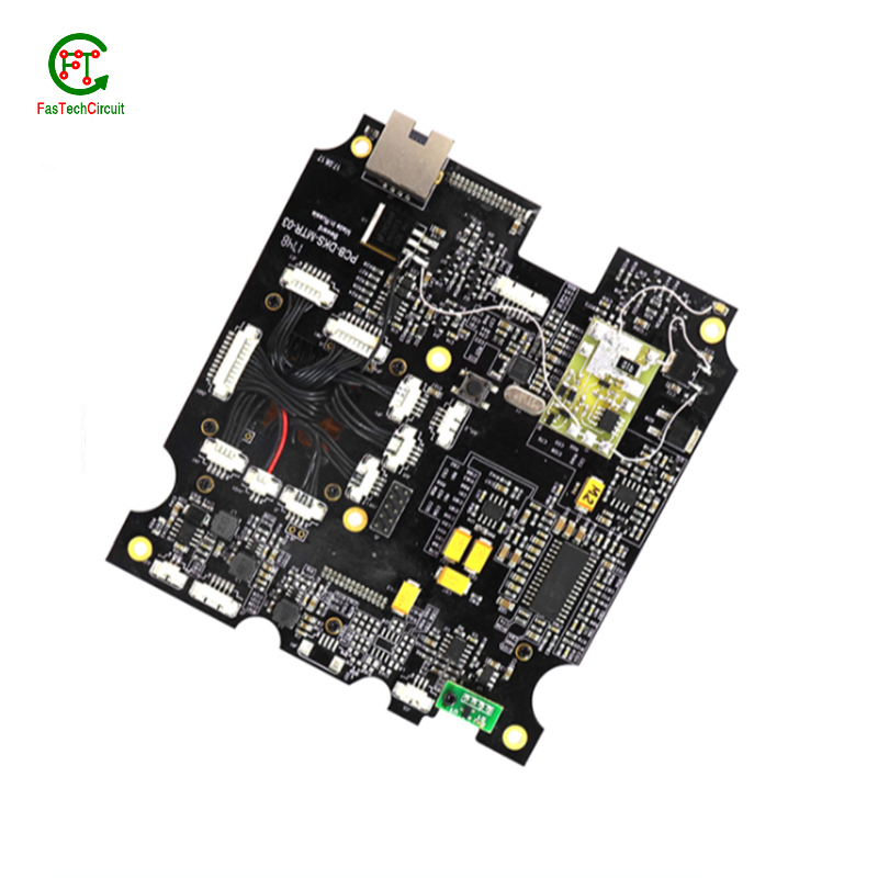
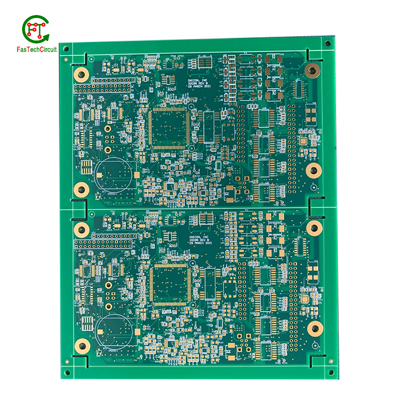
94v0 pcb 1-layer pcb board bearings FAQs Guide Welcome to our state-of-the-art PCB (Printed Circuit Board) products. We are proud to offer a comprehensive range of high-quality and versatile PCB solutions to meet the constantly evolving needs of the modern electronics industry.Our PCBs are expertly designed and manufactured using the latest technology and advanced techniques, ensuring reliability, durability, and exceptional performance for a wide range of applications. We understand the importance of precision and attention to detail in the production of PCBs and we are committed to meeting stringent quality standards.
2.What types of 94v0 pcb 1-layer pcb boards are there?
3.What is the difference between single-sided, double-sided, and multi-layer 94v0 pcb 1-layer pcb board?
4.Can a 94v0 pcb 1-layer pcb board be used for both power and signal transmission?
5.What is a through-hole component?
6.What software is used for 94v0 pcb 1-layer pcb board design?
7.How are high-frequency signals handled on a 94v0 pcb 1-layer pcb board?
8.What is the role of a data sheet in 94v0 pcb 1-layer pcb board design?
9.What is the maximum operating temperature of a 94v0 pcb 1-layer pcb board?
10.How are 94v0 pcb 1-layer pcb boards tested for quality control?
11.Are 94v0 pcb 1-layer pcb board recyclable?
12.What does 94v0 pcb 1-layer pcb board stand for?
13.What techniques are used for reducing electromagnetic interference (EMI) on a 94v0 pcb 1-layer pcb board?
14.What is the difference between a gold-plated and a tin-plated 94v0 pcb 1-layer pcb board?
15.How does a 94v0 pcb 1-layer pcb board work?
16.What is the minimum thickness of a 94v0 pcb 1-layer pcb board?
17.How are high-speed/high-frequency 94v0 pcb 1-layer pcb board tested and validated?
1.Can a 94v0 pcb 1-layer pcb board be used with both through-hole and surface mount components?
We continue to improve 94v0 pcb 1-layer pcb board products and processes to improve efficiency.
Yes, a PCB (printed circuit board) can be designed to accommodate both through-hole and surface mount components. This is known as a mixed-technology PCB. The PCB will have both through-hole and surface mount pads and traces, allowing for the placement and soldering of both types of components. This type of PCB is commonly used in electronic devices that require a combination of through-hole and surface mount components for functionality.
2.What types of 94v0 pcb 1-layer pcb boards are there?
As one of the 94v0 pcb 1-layer pcb board market leaders, we are known for innovation and reliability.
There are several types of PCBs, including single-sided, double-sided, multi-layer, and flexible PCBs. Single-sided PCBs have components mounted on one side and conductive traces on the other. Double-sided PCBs have components mounted on both sides with conductive traces connecting them. Multi-layer PCBs have several layers of conductive traces and insulating material sandwiched together. Flexible PCBs are made from a flexible plastic material, allowing them to bend and twist for use in applications where traditional rigid PCBs are not suitable. Each type of PCB serves a different purpose and can be used in a variety of electronic devices and applications.
3.What is the difference between single-sided, double-sided, and multi-layer 94v0 pcb 1-layer pcb board?
We have established a good reputation and reliable partnerships within the 94v0 pcb 1-layer pcb board industry.
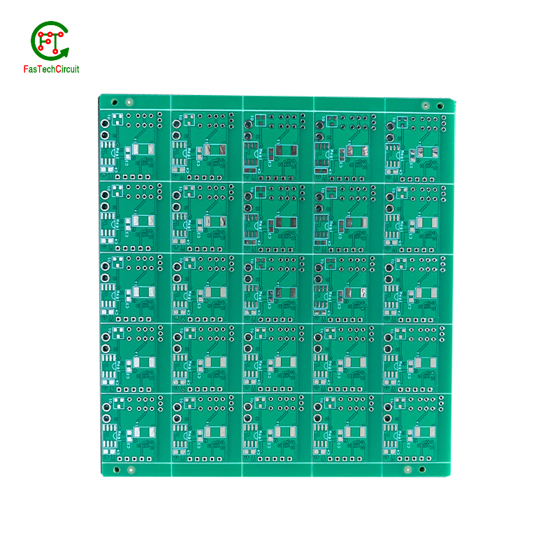
Single-sided PCB (Printed Circuit Board) is a type of PCB that has components and traces on only one side of the board. The other side is usually used for soldering and mounting the board onto a larger circuit.
Double-sided PCB is a type of PCB that has components and traces on both sides of the board. The traces on both sides are connected through vias, which are small holes drilled through the board and plated with metal to create an electrical connection.
Multi-layer PCB is a type of PCB that has multiple layers of conductive material and insulating material sandwiched together. The layers are connected through vias, allowing for more complex and compact circuit designs. Multi-layer PCBs are used in more advanced and high-performance electronic devices.
4.Can a 94v0 pcb 1-layer pcb board be used for both power and signal transmission?
Yes, a PCB (printed circuit board) can be used for both power and signal transmission. This is commonly seen in electronic devices such as computers, smartphones, and other electronic devices. The PCB acts as a platform for connecting various components and circuits, including power sources and signal pathways. The power and signal traces on the PCB are designed to handle different levels of current and voltage to ensure efficient transmission and prevent interference between the two. However, it is important to properly design and layout the PCB to ensure proper separation and isolation of power and signal traces to avoid any potential issues.
5.What is a through-hole component?
We focus on providing high 94v0 pcb 1-layer pcb board quality products and services.
A through-hole component is an electronic component that has leads or pins that are inserted into holes on a printed circuit board (PCB) and then soldered to the opposite side of the board. This type of component is typically larger and more robust than surface mount components, and is often used for high-power or high-voltage applications. Through-hole components are also easier to replace or repair compared to surface mount components.
6.What software is used for 94v0 pcb 1-layer pcb board design?
Our 94v0 pcb 1-layer pcb board products have competitive and differentiated advantages, and actively promote digital transformation and innovation.
Some popular software used for PCB design include:
1. Altium Designer
2. Eagle PCB
3. KiCad
4. OrCAD
5. PADS
6. Proteus
7. DipTrace
8. EasyEDA
9. CircuitMaker
10. DesignSpark PCB
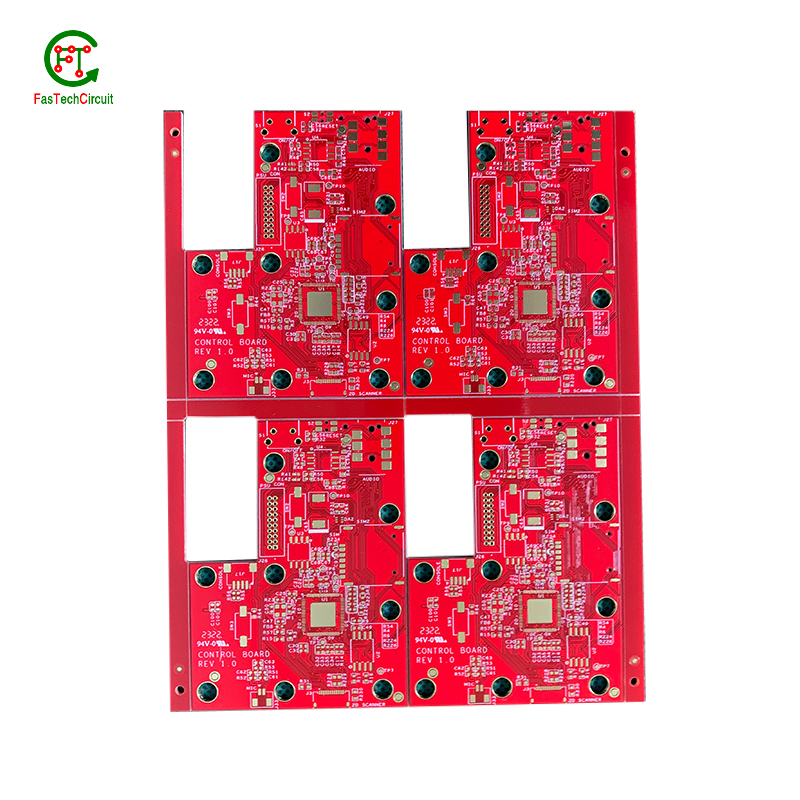
7.How are high-frequency signals handled on a 94v0 pcb 1-layer pcb board?
High-frequency signals are typically handled with great care and precision on a PCB to ensure optimal performance. This involves using high-quality materials, such as high-speed laminates and low-loss dielectrics, to minimize signal loss and interference. Additionally, designers must carefully consider the trace routing and placement of components on the PCB to minimize signal reflections and keep the signal path as short and direct as possible. Specialized techniques, like controlled impedance and shielding, may also be used to further improve signal integrity.
8.What is the role of a data sheet in 94v0 pcb 1-layer pcb board design?
A data sheet is an essential tool for PCB design, providing vital information and specifications for all of the components used in the design process. It contains detailed technical data, such as dimensions, electrical ratings, and performance characteristics, that allow designers to make informed decisions when selecting and placing components on a PCB. By referencing the data sheet, designers can ensure that each component is properly integrated into the overall design, following any necessary guidelines or restrictions. Additionally, data sheets also provide necessary information for the layout and routing of traces on the PCB, ensuring that the design can meet required performance specifications.
9.What is the maximum operating temperature of a 94v0 pcb 1-layer pcb board?
We have a professional team that is committed to the innovation and development of 94v0 pcb 1-layer pcb board.
The maximum operating temperature of a PCB (printed circuit board) can vary depending on the materials and components used in its construction. Generally, the maximum operating temperature for a standard FR4 PCB is around 130-140 degrees Celsius. However, specialized materials such as high-temperature laminates or ceramic substrates can withstand higher temperatures up to 200-250 degrees Celsius. The maximum operating temperature of a PCB should always be determined by the manufacturer's specifications and guidelines.
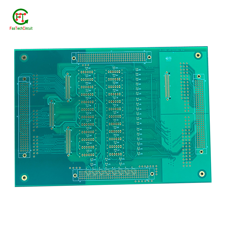
10.How are 94v0 pcb 1-layer pcb boards tested for quality control?
We have broad development space in domestic and foreign markets. 94v0 pcb 1-layer pcb board have great advantages in terms of price, quality, and delivery date.
PCB (Printed Circuit Board) testing is a critical step in the quality control process of electronic products. It ensures that all components and connections on the board are functioning correctly and that the PCB meets the required standards and specifications.
The testing process typically starts with a visual inspection to identify any visible defects, such as incorrect soldering or damaged components. Next, electrical testing is conducted to check the functionality of each individual component and the overall circuit.
One common method of testing is the use of a test fixture, which applies signals to the PCB and checks for correct responses. Other methods include automated optical inspection (AOI) and in-circuit testing (ICT).
Once the initial testing is completed, the PCB may undergo environmental testing to simulate real-life conditions and ensure its reliability and durability. This includes temperature and humidity cycling, vibration and shock testing, and more.
11.Are 94v0 pcb 1-layer pcb board recyclable?
We have been working hard to improve service quality and meet customer needs.
Yes, PCBs (printed circuit boards) are recyclable. They can be broken down and the individual components can be reused or repurposed. However, the recycling process can be complex and requires specialized equipment and techniques. It is important to properly dispose of PCBs to prevent environmental contamination and health hazards.
12.What does 94v0 pcb 1-layer pcb board stand for?
We attach importance to the innovation ability and team spirit of employees, have advanced R & D facilities and laboratories, and have a good quality management system.
PCB stands for Printed Circuit Board.
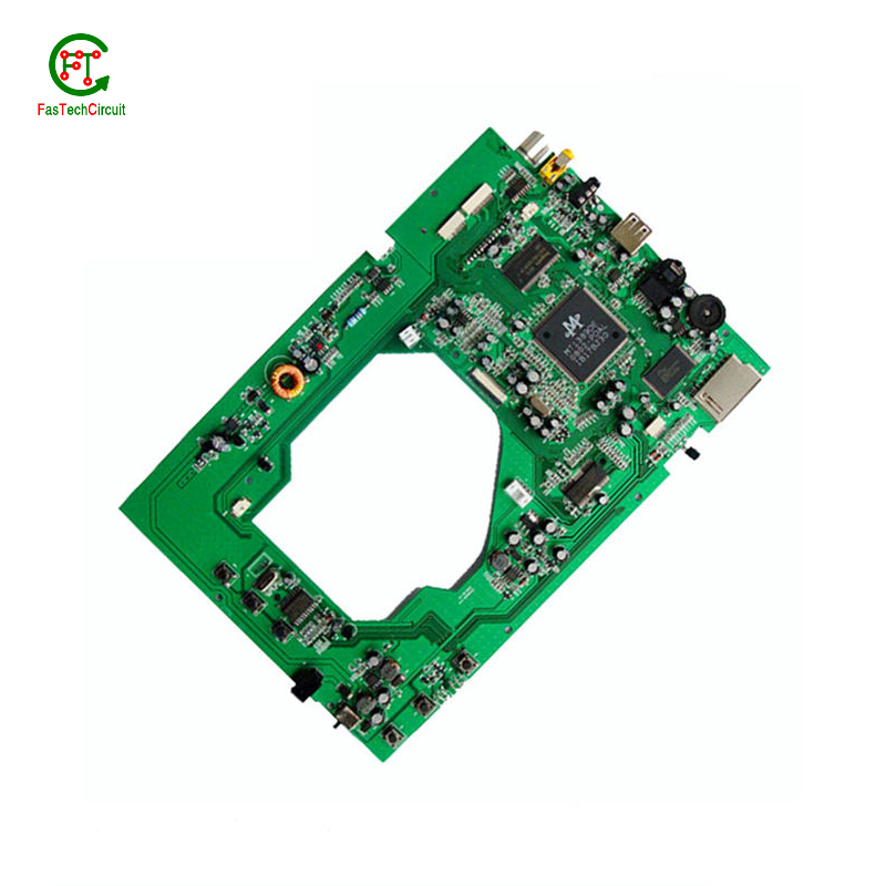
13.What techniques are used for reducing electromagnetic interference (EMI) on a 94v0 pcb 1-layer pcb board?
Electromagnetic interference (EMI) is a disturbance caused by electromagnetic radiation that can disrupt the proper functioning of electronic devices. To reduce EMI on a PCB, a number of techniques can be employed. One common technique is to use a ground plane, which acts as a shield to block electromagnetic waves from interfering with the circuit. Another approach is to use proper placement and routing of components and traces to minimize the length of signal paths and reduce the chances of signal crossover. Additionally, using components like capacitors and ferrite beads can help to filter out high-frequency noise. Careful consideration and design of the PCB layout is also crucial in reducing EMI, as the placement, size, and orientation of components can impact electromagnetic emissions. By employing these techniques, EMI on a PCB can be effectively reduced, leading to improved performance and reliability of electronic devices.
14.What is the difference between a gold-plated and a tin-plated 94v0 pcb 1-layer pcb board?
A gold-plated PCB (Printed Circuit Board) is a type of PCB that has a thin layer of gold coating on its surface. This layer is added through a process called electroplating and is commonly used to protect the PCB components from corrosion and increase the conductivity. On the other hand, a tin-plated PCB has a layer of tin coating on its surface, which is also applied through electroplating. Unlike gold plating, tin plating is mainly used to prevent oxidization and improve solderability.
15.How does a 94v0 pcb 1-layer pcb board work?
We maintain a stable growth through reasonable capital operations, focus on industry development trends and cutting -edge technologies, and focus on product quality and safety performance.
A PCB (Printed Circuit Board) is a thin board made of non-conductive material, such as fiberglass or plastic, with conductive pathways etched or printed onto its surface. These pathways, also known as traces, are used to connect electronic components on the board, such as resistors, capacitors, and integrated circuits.
The PCB works by providing a platform for the components to be mounted and connected in a specific circuit configuration. The traces on the board act as wires, allowing electricity to flow between the components and creating a complete circuit.
The process of creating a PCB involves several steps, including designing the circuit layout, printing or etching the traces onto the board, and attaching the components using soldering techniques. Once the components are attached, the board is tested to ensure that all connections are correct and functioning properly.
When a PCB is connected to a power source, electricity flows through the traces, powering the components and allowing them to perform their intended functions. The traces also act as a pathway for signals to travel between components, allowing for communication and data transfer within the circuit.
PCBs are used in a wide range of electronic devices, from simple household appliances to complex computer systems. They provide a compact and efficient way to connect and control electronic components, making them an essential part of modern technology.
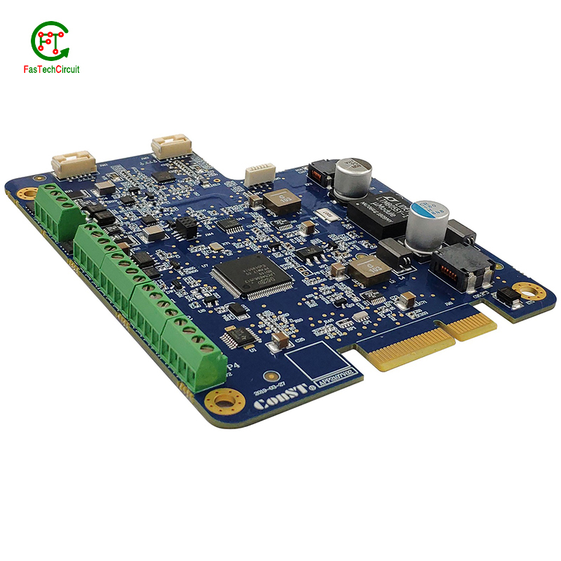
16.What is the minimum thickness of a 94v0 pcb 1-layer pcb board?
We are committed to providing personalized solutions and established long -term strategic cooperative relationships with customers.
The minimum thickness of a PCB (printed circuit board) can vary depending on the materials and manufacturing processes used. However, the standard minimum thickness for a single-sided PCB is 0.6mm (0.024 inches) and for a double-sided PCB it is 0.8mm (0.032 inches). Thinner PCBs can be made, but they may be more fragile and have limitations on the components and circuitry that can be used.
17.How are high-speed/high-frequency 94v0 pcb 1-layer pcb board tested and validated?
Testing and validation are essential steps in the production process of high-speed and high-frequency printed circuit boards (PCBs). These specialized types of PCBs are used in a wide range of industries, including telecommunications, aerospace, and automotive, and require precision and reliability in their performance.
The testing and validation process for high-speed/high-frequency PCBs involves several steps to ensure that the final product meets the required specifications. This starts with design simulation and analysis using specialized software to verify the layout and electrical characteristics of the PCB.
Once the design is confirmed, prototype PCBs are manufactured and subjected to various tests, including signal integrity and power integrity tests. These tests evaluate the electrical performance of the PCB, such as its ability to transmit signals at high speeds and maintain signal integrity.
In addition to electrical tests, environmental and mechanical tests are also performed to assess the durability and reliability of the PCB under different conditions, such as temperature changes and mechanical stress.
The final step in the testing and validation process is the inspection and analysis of the tested PCBs. This involves a detailed review of the test results and any necessary modifications to meet the required specifications.
RELATED PRODUCTS & SERVICE
pcb board manufacturing How To Contact US
PCB from 1 to 30 layers, HDI, Heavy Copper, Rigid-flex board with "pcb board manufacturing One-Stop" service.

