HDI PCB Circuit Board Medical PCB & PCBA Motherboard PCB Assembly with Components with High Quality and Low Price
Categories: All Products,pcb board manufacturing,PCB assembly
product categories.
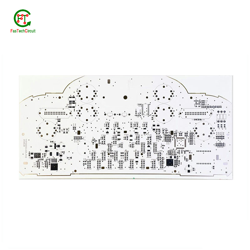
This is a PCB sample-09872, If you need other model pcb, please check our product categories.
Please email us for the pcb pricing ! if you would like to read it before placing your order.
The basic details are as follows:
| Type | 12 layer PCB |
| Place of Origin | Guangdong, China |
| Brand Name | FasTechCircuit PCB |
| Base Material | FR4 |
| Copper Thickness | 1oz |
| Board Thickness | 1.6mm |
| Min. Hole Size | 0.1mm |
| Min. Line Width | 0.075mm |
| Min. Line Spacing | 0.075mm |
| Surface Finishing | LF H AL |
| Board Size | 98 X 142 MM |
| Layers | 12 |
| Certification | ISO/RoHS/TS16949 |
| Silk Screen Min Line Width | 0.1mm |
| Silkscreen color | green,red,blue,white,black,yellow,etc. |
| Application | telecom,IOT,RF,smartcontrol,security,medical,industrial,automotive,3G/4G/5G products. |
| keywords | pcb board, PCB assembly |
| Min solder bridge | 3 mil |
| Minimum annular ring | 4 mil |
| Tolerance of back drill | +/-0.05mm |
| QC test | 100% test |
Tags:PCB,PCBA,HIGH SPEED PCB,MULTILAYER PCB,HDI PCB BOARD,RIGID-FLEX PCB,PCB ASSEMBLY,IMPEDANCE PCB,STANDARD PCB,SPECIAL PCB,FPC
Categories: All Products,IMPEDANCE PCB
What we can do?
pcb board manufacturing capability and services:
1. Single-sided, double side & multi-layer PCB. FPC. Flex Rigid PCB with competitive price,
good quality and excellent service.
2. CEM-1, CEM-3 FR-4, FR-4 High TG, Aluminum base material, Polyimide, etc.
3. HAL, HAL lead free, Immersion Gold/ Silver/Tin, OSP surface treatment.
4. Quantities range from sample to mass order
5. 100% E-Test
SMT(Surface Mounting technology),DIP.
1. Material Sourcing Service
2. SMT assembly and Through hole components insertion
3.100% AOI testing
4. IC pre-programming / Burning on-line
5.ICT testing
6.Function testing as requested
7.Complete Unit assembly (which including plastics, metal box, Coil, cable inside etc)
8.Conformal coating
9.OEM/ODM also welcomed
FAQ:
1. What are the materials used for making PCB?
The common materials used for making PCB include copper clad laminate, copper foil, solder mask, and silkscreen.
2. What is the purpose of a solder mask on a PCB?
The solder mask is a layer of protective coating that is applied to a PCB to protect the copper traces from corrosion and damage during the soldering process.
3. What is the difference between single-sided and double-sided PCB?
Single-sided PCB has only one layer of conductive material while double-sided PCB has conductive material on both sides, allowing for more complex circuit designs.
4. What are the benefits of using PCB in electronic devices?
Using PCB in electronic devices offers several benefits such as compact design, increased reliability, easier repair and maintenance, and reduced production costs.
5. What is the role of traces on a PCB?
Traces are conductive pathways etched onto the surface of a PCB, they serve as the connections between different components, allowing for the flow of electricity.
6. Can PCB be recycled?
Yes, PCB can be recycled to recover valuable materials such as copper and gold, reducing the environmental impact of electronic waste.
7. What is the maximum current a PCB can handle?
The maximum current a PCB can handle depends on its size, thickness, and the type of material used. It is important to consult the manufacturer's specifications for the specific PCB being used.
8. How are components attached to a PCB?
Components are attached to a PCB through different methods such as soldering, surface mount technology, and through-hole technology.
9. What is the difference between through-hole and surface mount technology?
Through-hole technology involves inserting component leads through holes on the PCB and soldering them in place, while surface mount technology involves soldering components directly onto the surface of the PCB.
10. Can PCB be customized for specific applications?
Yes, PCBs can be customized to fit specific design requirements, allowing for unique and optimized functionality in electronic devices.
11. What is the typical lifespan of a PCB?
The lifespan of a PCB largely depends on the quality of materials and production processes used. On average, a well-manufactured PCB can last up to 10 years or more.
12. Can PCB be used for high-frequency applications?
Yes, PCBs can be designed and manufactured to handle high-frequency signals, making them suitable for use in devices such as smartphones and wireless communication devices.
13. How are PCBs tested for quality?
PCB undergo a series of tests such as visual inspection, continuity testing, and functional testing to ensure they meet quality standards and function properly.
14. Can PCB be repaired if they are damaged?
In some cases, PCBs can be repaired by replacing faulty components or repairing damaged traces. However, it is often more efficient to replace the entire PCB.
15. What is the role of silkscreen on a PCB?
Silkscreen is a layer of ink printed onto a PCB that displays information such as component labels, reference numbers, and logos, providing visual aid for assembly and troubleshooting.
RELATED PRODUCTS & SERVICE


pcb board manufacturing How To Contact US
PCB from 1 to 30 layers, HDI, Heavy Copper, Rigid-flex board with "pcb board manufacturing One-Stop" service.