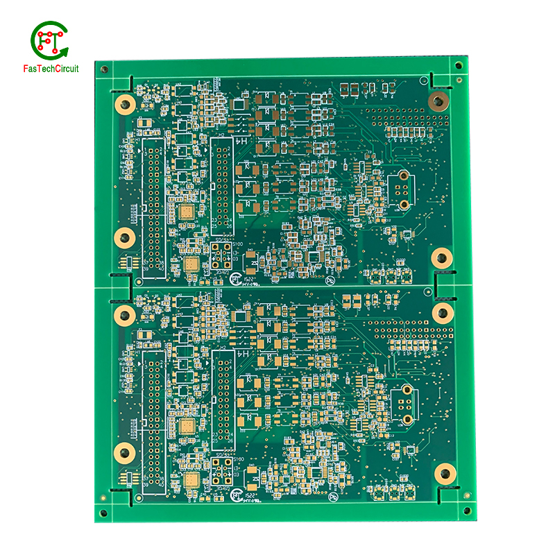
8layers pcb board
| Model Number | customized PCBA |
| Type | pcba |
| Place of Origin | Guangdong, China |
| Brand Name | none |
| Copper Thickness | 1 oz |
| Supplier Type | OEM |
| Application | Electronics Device |
| Service | One-step Service |
| Layer | 1-33layers |
| Solder mask color | Blue.green.red.black.white.etc |
| Testing Service | 100% |
| Component size | 0201-1176mm |
| Component max height | 16mm |
| Min lead pitch | 0.1mm |
| Min BGA ball pitch | 0.6mm |
| Max PCB size | 451x522mm |
| Packaging Details | Vacuum package for bare PCB and ESD package for PCBA Printed Circuit Board Factory FPC Board PCBA Companies PCBA Assembly |
| Supply Ability | 43822 Piece/Pieces per Week |
| Quantity (pieces) | > 760 |
| Lead time (days) | 14 |
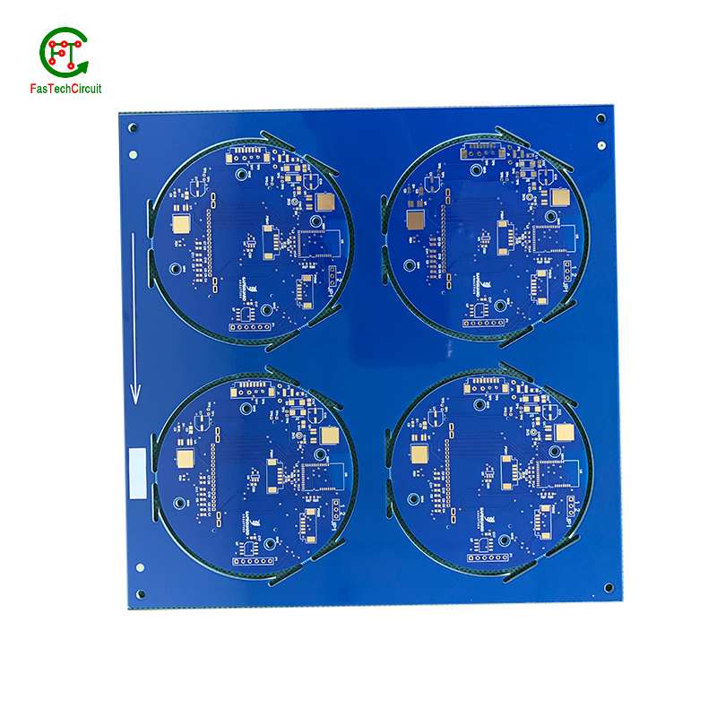
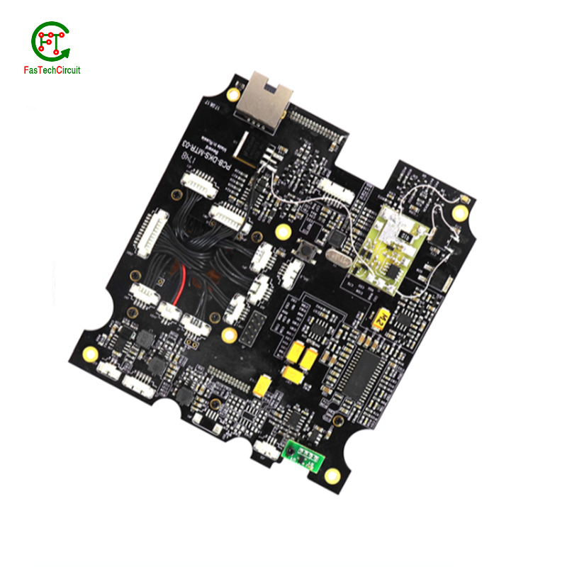
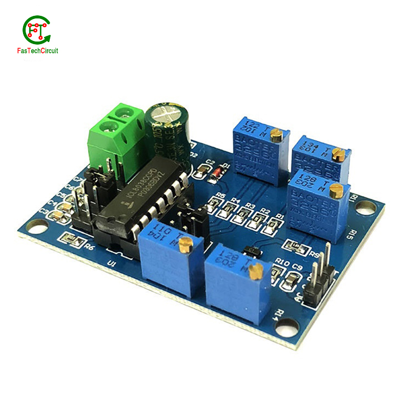
8layers pcb board bearings FAQs Guide Welcome to our state-of-the-art PCB (Printed Circuit Board) products. We are proud to offer a comprehensive range of high-quality and versatile PCB solutions to meet the constantly evolving needs of the modern electronics industry.Our PCBs are expertly designed and manufactured using the latest technology and advanced techniques, ensuring reliability, durability, and exceptional performance for a wide range of applications. We understand the importance of precision and attention to detail in the production of PCBs and we are committed to meeting stringent quality standards.
2.What is the difference between a gold-plated and a tin-plated 8layers pcb board?
3.What type of material is used for the silkscreen on a 8layers pcb board?
4.What is the maximum operating temperature of a 8layers pcb board?
5.How does a 8layers pcb board work?
6.How are 8layers pcb boards protected from environmental factors?
7.What are the benefits of using surface mount technology (SMT) for 8layers pcb board?
8.What is the purpose of a 8layers pcb board?
9.What techniques are used for reducing electromagnetic interference (EMI) on a 8layers pcb board?
10.How are 8layers pcb boards tested for quality control?
11.What is the purpose of a ground plane on a 8layers pcb board?
12.What is the role of vias on a 8layers pcb board?
13.How are through-hole components soldered onto a 8layers pcb board?
14.How are thermal considerations taken into account during 8layers pcb board design?
15.What is the typical lifespan of a 8layers pcb board?
1.Can 8layers pcb boards be customized?
We should enjoy a good reputation in the industry, and we can increase the added value of the products of cooperative customers through technological innovation.
Yes, PCBs (printed circuit boards) can be customized to meet specific design requirements. This can include changes to the size, shape, number of layers, and placement of components on the board. Customization can also involve the use of specialized materials, finishes, and manufacturing processes to meet specific performance or environmental requirements. PCB manufacturers often offer design services to help customers create custom PCBs that meet their unique needs.
2.What is the difference between a gold-plated and a tin-plated 8layers pcb board?
A gold-plated PCB (Printed Circuit Board) is a type of PCB that has a thin layer of gold coating on its surface. This layer is added through a process called electroplating and is commonly used to protect the PCB components from corrosion and increase the conductivity. On the other hand, a tin-plated PCB has a layer of tin coating on its surface, which is also applied through electroplating. Unlike gold plating, tin plating is mainly used to prevent oxidization and improve solderability.
3.What type of material is used for the silkscreen on a 8layers pcb board?
We have a wide range of 8layers pcb board customer groups and establishes long -term cooperative relationships with partners. The countries we provide services include .
The material used for the silkscreen on a PCB is typically a white or black ink made of epoxy or acrylic. It is applied using a screen printing process and is cured at high temperatures to ensure durability and resistance to chemicals and solvents.
4.What is the maximum operating temperature of a 8layers pcb board?
We have a professional team that is committed to the innovation and development of 8layers pcb board.
The maximum operating temperature of a PCB (printed circuit board) can vary depending on the materials and components used in its construction. Generally, the maximum operating temperature for a standard FR4 PCB is around 130-140 degrees Celsius. However, specialized materials such as high-temperature laminates or ceramic substrates can withstand higher temperatures up to 200-250 degrees Celsius. The maximum operating temperature of a PCB should always be determined by the manufacturer's specifications and guidelines.
5.How does a 8layers pcb board work?
We maintain a stable growth through reasonable capital operations, focus on industry development trends and cutting -edge technologies, and focus on product quality and safety performance.
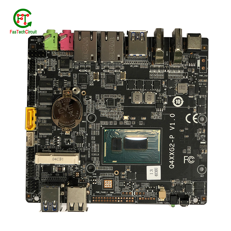
A PCB (Printed Circuit Board) is a thin board made of non-conductive material, such as fiberglass or plastic, with conductive pathways etched or printed onto its surface. These pathways, also known as traces, are used to connect electronic components on the board, such as resistors, capacitors, and integrated circuits.
The PCB works by providing a platform for the components to be mounted and connected in a specific circuit configuration. The traces on the board act as wires, allowing electricity to flow between the components and creating a complete circuit.
The process of creating a PCB involves several steps, including designing the circuit layout, printing or etching the traces onto the board, and attaching the components using soldering techniques. Once the components are attached, the board is tested to ensure that all connections are correct and functioning properly.
When a PCB is connected to a power source, electricity flows through the traces, powering the components and allowing them to perform their intended functions. The traces also act as a pathway for signals to travel between components, allowing for communication and data transfer within the circuit.
PCBs are used in a wide range of electronic devices, from simple household appliances to complex computer systems. They provide a compact and efficient way to connect and control electronic components, making them an essential part of modern technology.
6.How are 8layers pcb boards protected from environmental factors?
We have established long-term and stable partnerships with our suppliers, so we have great advantages in price and cost and quality assurance.
PCBs, or printed circuit boards, are protected from environmental factors through the use of various techniques and materials. One method is to coat the PCB with a layer of conformal coating, which is a thin layer of protective material that covers the components and circuitry on the board. This coating can protect the PCB from moisture, dust, and other contaminants that could cause damage.
In addition to conformal coating, PCBs can also be protected through designing the layout of the board in a way that minimizes exposure to environmental factors. This includes placing sensitive components in areas that are less susceptible to moisture or temperature changes, as well as using specialized materials that are resistant to the effects of heat, humidity, and other environmental conditions.
7.What are the benefits of using surface mount technology (SMT) for 8layers pcb board?
We focus on innovation and continuous improvement to maintain a competitive advantage.
Surface mount technology (SMT) is a popular method for assembling printed circuit boards (PCBs) that offers numerous benefits over traditional through-hole components. Firstly, SMT components are smaller and more compact, allowing for greater PCB density and reducing the overall size of the board. This makes SMT ideal for increasingly miniaturized electronics, such as smartphones and wearables. Additionally, SMT components are typically cheaper and easier to manufacture, leading to cost savings in both materials and labor. SMT also allows for automated assembly, resulting in faster and more efficient production processes. Furthermore, the smaller size of SMT components leads to improved electrical performance due to decreased parasitic effects and shorter signal paths. This makes SMT ideal for high-frequency applications.
8.What is the purpose of a 8layers pcb board?
We pay attention to the transformation of intellectual property protection and innovation achievements. Your OEM or ODM order design we have a complete confidentiality system.
A PCB (Printed Circuit Board) is a flat board made of non-conductive material, such as fiberglass, with conductive pathways etched or printed onto it. The main purpose of a PCB is to provide a platform for electronic components to be mounted and connected together to form a functioning electronic circuit. It serves as a physical support for the components and provides a means for them to communicate with each other through the conductive pathways. PCBs are used in a wide range of electronic devices, from simple household appliances to complex computer systems, and are essential for the proper functioning and reliability of these devices. They also allow for easier and more efficient production of electronic devices, as the components can be mounted and connected in a standardized and automated manner.
9.What techniques are used for reducing electromagnetic interference (EMI) on a 8layers pcb board?
Electromagnetic interference (EMI) is a disturbance caused by electromagnetic radiation that can disrupt the proper functioning of electronic devices. To reduce EMI on a PCB, a number of techniques can be employed. One common technique is to use a ground plane, which acts as a shield to block electromagnetic waves from interfering with the circuit. Another approach is to use proper placement and routing of components and traces to minimize the length of signal paths and reduce the chances of signal crossover. Additionally, using components like capacitors and ferrite beads can help to filter out high-frequency noise. Careful consideration and design of the PCB layout is also crucial in reducing EMI, as the placement, size, and orientation of components can impact electromagnetic emissions. By employing these techniques, EMI on a PCB can be effectively reduced, leading to improved performance and reliability of electronic devices.
10.How are 8layers pcb boards tested for quality control?
We have broad development space in domestic and foreign markets. 8layers pcb board have great advantages in terms of price, quality, and delivery date.
PCB (Printed Circuit Board) testing is a critical step in the quality control process of electronic products. It ensures that all components and connections on the board are functioning correctly and that the PCB meets the required standards and specifications.
The testing process typically starts with a visual inspection to identify any visible defects, such as incorrect soldering or damaged components. Next, electrical testing is conducted to check the functionality of each individual component and the overall circuit.
One common method of testing is the use of a test fixture, which applies signals to the PCB and checks for correct responses. Other methods include automated optical inspection (AOI) and in-circuit testing (ICT).
Once the initial testing is completed, the PCB may undergo environmental testing to simulate real-life conditions and ensure its reliability and durability. This includes temperature and humidity cycling, vibration and shock testing, and more.
11.What is the purpose of a ground plane on a 8layers pcb board?
I have a comprehensive after -sales service system, which can pay attention to market trends in time and adjust our strategy in a timely manner.
A decoupling capacitor is an essential component on a PCB (Printed Circuit Board) which is used to reduce or eliminate high frequency noise between different components. It acts as a buffer between the power supply and other circuit components, by storing electrical charge and then releasing it when there is a sudden change in the supply voltage. This helps to stabilize the power supply, providing a steady and noise-free flow of electricity to the circuit. Furthermore, decoupling capacitors also help to filter out any unwanted signals that may cause interference or disruptions in the proper functioning of the circuit.
12.What is the role of vias on a 8layers pcb board?
Our company has many years of 8layers pcb board experience and expertise.
Vias play a crucial role in connecting different layers of a printed circuit board (PCB). These small, plated holes act as conductive paths, allowing signals and power to pass through the board and reach various components. Vias are also essential for routing traces from one layer to another, optimizing the layout and reducing the size and complexity of the board. Additionally, vias provide structural support and improve thermal management by facilitating heat dissipation.
13.How are through-hole components soldered onto a 8layers pcb board?
Through-hole components are soldered onto a printed circuit board (PCB) using a process called wave soldering. First, the PCB is fitted with all the necessary through-hole components, such as resistors, capacitors, and diodes. Then, the board is passed over a wave of molten solder, which flows through the holes in the PCB and creates a secure connection between the component and the board. The excess solder is removed and the board is inspected to ensure all components are properly soldered. This method of soldering provides a strong and reliable connection for through-hole components, making it a popular choice for electronic assembly.
14.How are thermal considerations taken into account during 8layers pcb board design?
As one of the top 8layers pcb board manufacturers in China, we take this very seriously.
Thermal considerations are crucial in the design of printed circuit boards (PCB), as excessive heat can greatly affect the performance and lifespan of electronic components. PCB design engineers must carefully consider thermal management strategies, such as proper placement of heat-generating components, effective heat dissipation techniques, and optimal selection of materials. Thermal simulations and analysis are also commonly used to evaluate and optimize the PCB design to ensure that the temperature of the PCB and its components are within safe limits. By taking into account these thermal considerations, the finished PCB can perform reliably and efficiently, ensuring the overall quality and function of electronic devices.
15.What is the typical lifespan of a 8layers pcb board?
8layers pcb board is not a product only, but also can help you comes to money-making.
The typical lifespan of a PCB (printed circuit board) can vary greatly depending on various factors such as the quality of materials used, environmental conditions, and usage. In general, a well-designed and properly manufactured PCB can last for 10-20 years or more. However, some PCBs may fail prematurely due to factors such as corrosion, thermal stress, or mechanical damage. Regular maintenance and proper handling can also extend the lifespan of a PCB.
RELATED PRODUCTS & SERVICE
pcb board manufacturing How To Contact US
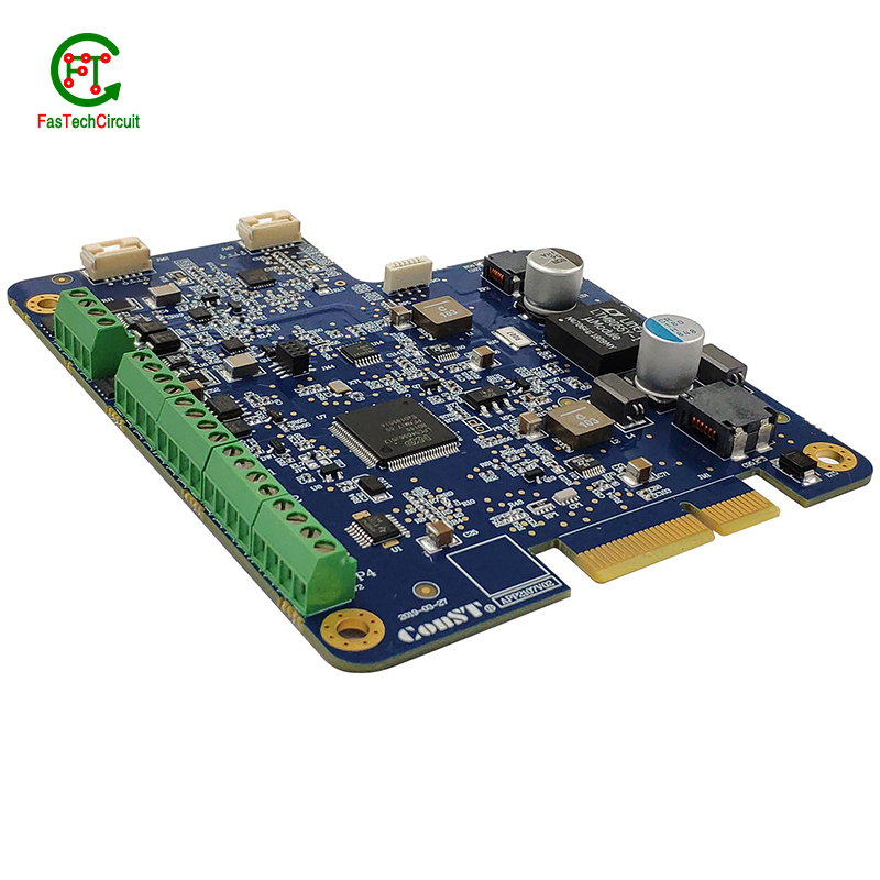
PCB from 1 to 30 layers, HDI, Heavy Copper, Rigid-flex board with "pcb board manufacturing One-Stop" service.

