PCB circuit board supplier
This is an article about PCB assembly process, for more information and products, please click below:
Categories: Details, All Products,PCB ASSEMBLY,PCB
PCB Development and Production Process Design
Advanced modern technology is advancing rapidly in various fields, and various industries around the world are developing at a very fast pace. The development of high-tech technology continues to affect our daily lives. Enjoying the achievements brought by technology has also brought about significant qualitative changes in our way of life. Various technological advancements have brought many advanced equipment to the world, which was unimaginable under the conditions of ancient decades ago. Especially for electronic components and electronic components, the core support of these devices is electronic engineering, and the core is printed circuit boards (PCBs).
PCB board is the support for electronic components, providing connections between electronic components and electrical appliances. PCB board is usually green and is a hard object plate that is fixed with various electronic components on this complex circuit board. These components with different division of labor are soldered onto the PCB during a process called "PCB assembly" or PCBA. PCB is made of glass fiber, which is not easy to bend and has insulation and heat insulation characteristics. It is composed of a substrate, components, copper layers for making traces, holes for installing components, and layers that can be inner and outer layers.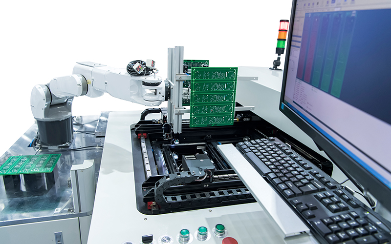
PCB board assembly process for electronic components
The advancement of electronic production technology has brought more possibilities for various difficult PCB assembly. There are currently three commonly used assembly techniques, the first being SMT, which is surface mount technology, the second being THT, which is through-hole technology, and the third being a combination of SMT and THT.
The PCB assembly process of components is established after the PCB is manufactured and formed, and the various required structures of the board are completely formed and manufactured according to customer requirements. The various components of PCB include operations such as template preparation and solder paste printing, placement of SMD parts, bonding formation in the curing furnace, and final inspection of PCB functionality. After preparing the required template, proceed with solder paste printing. At this stage of the printed board, strict consideration needs to be given to filling the small holes that provide installation points for electrical components with extremely high accuracy. Otherwise, the produced board may have some serious defects, such as mismatched bridge joints in the puzzle. Bridges on slabs usually have small dimensions and are not easily invisible to the naked eye. If the most advanced testing equipment is not used for testing, it is difficult to detect whether they are qualified. Nevertheless, they are still the most common and complex problems in the PCB assembly process, and once problems occur, they can easily lead to short circuits or even component burnout. Therefore, our FasTechCircuit adopts the latest printing technology to ensure that each printed circuit board can function properly at the end of the assembly line.
Another key part of the PCB assembly process is the use of a pick-up and drop machine to position electronic components. Each wire on the circuit board is very small and precise, and each wire must be perfectly aligned with the conductive part of the electronic component. Therefore, electronic devices must be fixed to the board with the highest accuracy and posted on the board. FasTechCircuit uses the most accurate three reference point optical system to place surface mounted devices. Finally, at the end of the PCB assembly line, a solid and stable connection between SMD and the board was achieved in the curing furnace. With the support of various advanced welding technologies, the service life and durability of printed circuit boards have been greatly improved, which is our ultimate goal in producing high-quality printed circuit boards.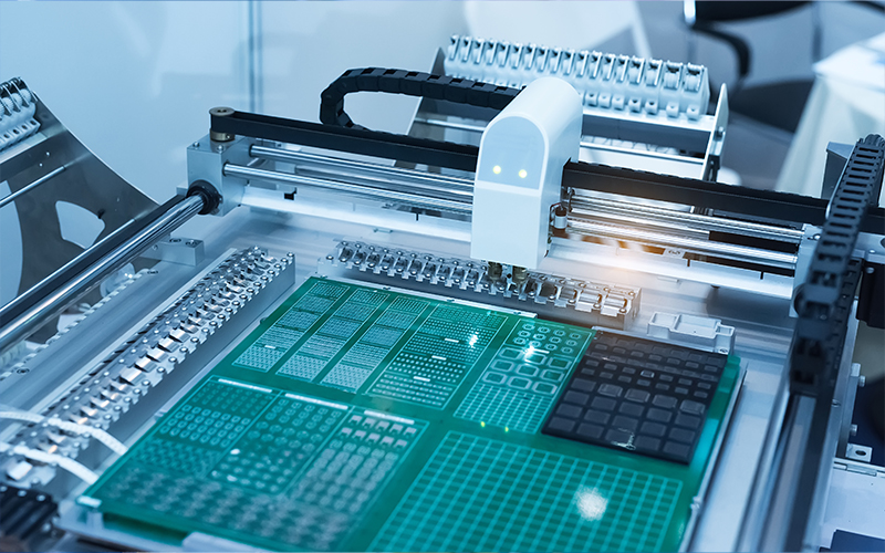
Specific requirements for printed circuit board components
There are multiple signal layers between the outer layers of the PCB board. The types and functions of each level are interrelated and independent, with the following 6 elements:
1. Layout of circuit board components: All components on the printed circuit board must be accurately placed on the fixed board and welded correctly in sequence and structure.
2. Printed circuit board solder joint quality: All solder joints on the circuit board must be clean and tidy, and the reliability of the solder joints must be monitored intelligently, without defects such as voids, bridging, or cold solder joints.
3. Positioning of circuit board components: All production circuit board components must be correctly positioned to avoid various errors, accurately placed and positioned to ensure the normal operation of the circuit board.
4. Safety performance electrical testing: Printed circuit boards must undergo strict and correct electrical operation testing to ensure the reliability of circuit board performance
5. Circuit board solder mask: All exposed copper on the circuit board must be covered with a protective coating to prevent oxidation and other damage to the circuit board and all components on the circuit board.
6. Circuit board cleaning: Before completing various performance tests and packaging, any solder residue attached to the circuit board must be cleaned.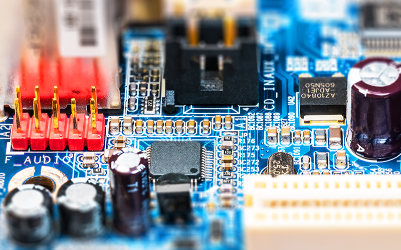
pcb board manufacturing How To Contact US
PCB from 1 to 30 layers, HDI, Heavy Copper, Rigid-flex board with "pcb board manufacturing One-Stop" service.